DP8573AVX/NOPB National Semiconductor, DP8573AVX/NOPB Datasheet - Page 3
DP8573AVX/NOPB
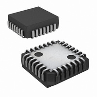
Manufacturer Part Number
DP8573AVX/NOPB
Description
IC REAL TIME CLOCK (RTC) 28-PLCC
Manufacturer
National Semiconductor
Type
Clock/Calendar/NVSRAMr
Datasheet
1.DP8573AVXNOPB.pdf
(16 pages)
Specifications of DP8573AVX/NOPB
Memory Size
32B
Time Format
HH:MM:SS:hh (12/24 hr)
Date Format
YY-MM-DD-dd
Interface
Parallel
Voltage - Supply
4.5 V ~ 5.5 V
Operating Temperature
-40°C ~ 85°C
Mounting Type
Surface Mount
Package / Case
28-PLCC
Bus Type
Parallel
Operating Supply Voltage (typ)
5V
Package Type
PLCC
Operating Supply Voltage (max)
5.5V
Operating Supply Voltage (min)
4.5V
Operating Temperature Classification
Industrial
Operating Temperature (max)
85C
Operating Temperature (min)
-40C
Pin Count
28
Mounting
Surface Mount
Lead Free Status / RoHS Status
Lead free / RoHS Compliant
Other names
*DP8573AVX
*DP8573AVX/NOPB
DP8573AVX
*DP8573AVX/NOPB
DP8573AVX
Available stocks
Company
Part Number
Manufacturer
Quantity
Price
Company:

Part Number:
DP8573AVX/NOPB
Manufacturer:
Texas Instruments
Quantity:
10 000


READ TIMING
WRITE TIMING
INTERRUPT TIMING
AC Electrical Characteristics
V
Note 8 Read Strobe width as used in the read timing table is defined as the period when both chip select and read inputs are low Hence read commences when
both signals are low and terminates when either signal returns high
Note 9 Hold time is guaranteed by design but not production tested This limit is not used to calculate outgoing quality levels
Note 10 Write Strobe width as used in the write timing table is defined as the period when both chip select and write inputs are low Hence write commences when
both signals are low and terminates when either signal returns high
AC Test Conditions
Note 11 C
Note 12 S1
Capacitance
Note 13 This parameter is not 100% tested
Note 14 Output rise and fall times 25 ns max (10%–90%) with 100 pF load
CC
Symbol
t
t
t
t
t
t
t
t
t
t
t
t
t
t
t
t
Symbol
C
C
AR
RW
CD
RAH
RD
DZ
RCH
DS
AW
WAH
CW
WW
DW
WDH
WCH
ROLL
Input Pulse Levels
Input Rise and Fall Times
Input and Output
Reference Levels
TRI-STATE Reference
Levels (Note 12)
IN
OUT
e
S1
S1
5V
L
e
e
e
e
g
V
GND for active high to high impedance measurements
open for all other timing measurements
100 pF includes jig and scope capacitance
CC
10% V
for active low to high impedance measurements
Input Capacitance
Output Capacitance
Parameter
BB
Address Valid Prior to Read Strobe
Read Strobe Width (Note 8)
Chip Select to Data Valid Time
Address Hold after Read (Note 9)
Read Strobe to Valid Data
Read or Chip Select to TRI-STATE
Chip Select Hold after Read Strobe
Minimum Inactive Time between Read or Write Accesses
Address Valid before Write Strobe
Address Hold after Write Strobe (Note 9)
Chip Select to End of Write Strobe
Write Strobe Width (Note 10)
Data Valid to End of Write Strobe
Data Hold after Write Strobe (Note 9)
Chip Select Hold after Write Strobe
Clock rollover to INTR out typically 16 5 s
(Note 14)
(T
A
e
e
3V V
25 C f
PFAIL l
e
Active High
Active Low
6 ns (10%–90%)
1 MHz)
GND to 3 0V
V
Typ
IH
5
7
Parameter
1 3V
C
L
b
a
e
0 5V
0 5V
Units
100 pF (unless otherwise specified)
pF
pF
3
Min
20
80
50
20
90
80
50
3
0
3
3
0
Max
80
70
60
TL F 9981 – 2
Units
ns
ns
ns
ns
ns
ns
ns
ns
ns
ns
ns
ns
ns
ns
ns
Related parts for DP8573AVX/NOPB
Image
Part Number
Description
Manufacturer
Datasheet
Request
R

Part Number:
Description:
IC REAL TIME CLOCK (RTC) 28-PLCC
Manufacturer:
National Semiconductor
Datasheet:

Part Number:
Description:
Clock IC
Manufacturer:
National Semiconductor
Datasheet:

Part Number:
Description:
National Semiconductor [8-Bit D/A Converter]
Manufacturer:
National Semiconductor
Datasheet:
Part Number:
Description:
National Semiconductor [Media Coprocessor]
Manufacturer:
National Semiconductor
Datasheet:
Part Number:
Description:
Digitally Controlled Tone and Volume Circuit with Stereo Audio Power Amplifier, Microphone Preamp Stage and National 3D Sound
Manufacturer:
National Semiconductor
Datasheet:
Part Number:
Description:
Digitally Controlled Tone and Volume Circuit with Stereo Audio Power Amplifier, Microphone Preamp Stage and National 3D Sound
Manufacturer:
National Semiconductor
Datasheet:
Part Number:
Description:
AC97 Rev 2 Codec with Sample Rate Conversion and National 3D Sound
Manufacturer:
National Semiconductor
Part Number:
Description:
Manufacturer:
National Semiconductor
Datasheet:
Part Number:
Description:
Manufacturer:
National Semiconductor
Datasheet:
Part Number:
Description:
General Purpose, Low Voltage, Low Power, Rail-to-Rail Output Operational Amplifiers
Manufacturer:
National Semiconductor
Datasheet:
Part Number:
Description:
8-bit 20 MSPS flash A/D converter.
Manufacturer:
National Semiconductor
Datasheet:
Part Number:
Description:
Low Noise Quad Operational Amplifier
Manufacturer:
National Semiconductor
Datasheet:
Part Number:
Description:
Quad Differential Line Receivers
Manufacturer:
National Semiconductor
Datasheet: