DP8573AVX/NOPB National Semiconductor, DP8573AVX/NOPB Datasheet - Page 4
DP8573AVX/NOPB
Manufacturer Part Number
DP8573AVX/NOPB
Description
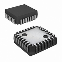
IC REAL TIME CLOCK (RTC) 28-PLCC
Manufacturer
National Semiconductor
Type
Clock/Calendar/NVSRAMr
Datasheet
1.DP8573AVXNOPB.pdf
(16 pages)
Specifications of DP8573AVX/NOPB
Memory Size
32B
Time Format
HH:MM:SS:hh (12/24 hr)
Date Format
YY-MM-DD-dd
Interface
Parallel
Voltage - Supply
4.5 V ~ 5.5 V
Operating Temperature
-40°C ~ 85°C
Mounting Type
Surface Mount
Package / Case
28-PLCC
Bus Type
Parallel
Operating Supply Voltage (typ)
5V
Package Type
PLCC
Operating Supply Voltage (max)
5.5V
Operating Supply Voltage (min)
4.5V
Operating Temperature Classification
Industrial
Operating Temperature (max)
85C
Operating Temperature (min)
-40C
Pin Count
28
Mounting
Surface Mount
Lead Free Status / RoHS Status
Lead free / RoHS Compliant
Other names
*DP8573AVX
*DP8573AVX/NOPB
DP8573AVX
*DP8573AVX/NOPB
DP8573AVX
Available stocks
Company
Part Number
Manufacturer
Quantity
Price
Company:

Part Number:
DP8573AVX/NOPB
Manufacturer:
Texas Instruments
Quantity:
10 000


Timing Waveforms
Pin Description
CS RD WR (Inputs) These pins interface to
lines The CS pin is an active low enable for the read and
write operations Read and Write pins are also active low
and enable reading or writing to the RTC All three pins are
disabled when power failure is detected However if a read
or write is in progress at this time it will be allowed to com-
plete its cycle
A0 –A4 (Inputs) These 5 pins are for register selection
They individually control which location is to be accessed
These inputs are disabled when power failure is detected
OSC IN (Input) OSC OUT (Output) These two pins are
used to connect the crystal to the internal parallel resonant
oscillator The oscillator is always running when power is
applied to V
MFO (Output) The multi-function output can be used as a
second interrupt (Power fail) output for interrupting the P
This pin can also provide an output for the oscillator The
MFO output is configured as push-pull active high for nor-
mal or single power supply operation and as an open drain
during standby mode (V
mode and a pull-up resistor is attached it should be con-
nected to a voltage no greater than V
INTR (Output) The interrupt output is used to interrupt the
processor when a timing event or power fail has occurred
and the respective interrupt has been enabled The INTR
output is permanently configured active low open drain If in
BB
and V
CC
BB l
V
CC
) If in battery backed
BB
P control
Write Timing Diagram
Read Timing Diagram
4
battery backed mode and a pull-up resistor is attached it
should be connected to a voltage no greater than V
output is a DC voltage level To clear the INTR write a 1 to
the appropriate bit(s) in the Main Status Register
D0– D7 (Input Output) These 8 bidirectional pins connect
to the host
write to the RTC When the PFAIL pin goes low and a write
is not in progress these pins are at TRI-STATE
PFAIL (Input) In battery backed mode this pin can have a
digital signal applied to it via some external power detection
logic When PFAIL
mode in a minimum of 30 s or a maximum of 63 s unless
lockout delay is programmed In the single power supply
mode this pin is not useable as an input and should be tied
to V
tion
V
up power supply This power supply is switched to the inter-
nal circuitry when the V
ing this pin eliminates the need for external logic to switch in
and out the back-up power supply If this feature is not to be
used then this pin must be tied to ground the RTC pro-
grammed for single power supply only and power applied to
the V
V
GND This is the common ground power pin for both V
and V
BB
CC
CC
(Battery Power Pin) This pin is connected to a back-
CC
This is the main system power pin
CC
Refer to section on Power Fail Functional Descrip-
pin
P’s data bus and are used to read from and
e
logic 0 the RTC goes into a lockout
CC
becomes lower than V
TL F 9981– 3
TL F 9981– 4
BB
BB
Utiliz-
The
BB
Related parts for DP8573AVX/NOPB
Image
Part Number
Description
Manufacturer
Datasheet
Request
R

Part Number:
Description:
IC REAL TIME CLOCK (RTC) 28-PLCC
Manufacturer:
National Semiconductor
Datasheet:

Part Number:
Description:
Clock IC
Manufacturer:
National Semiconductor
Datasheet:

Part Number:
Description:
National Semiconductor [8-Bit D/A Converter]
Manufacturer:
National Semiconductor
Datasheet:
Part Number:
Description:
National Semiconductor [Media Coprocessor]
Manufacturer:
National Semiconductor
Datasheet:
Part Number:
Description:
Digitally Controlled Tone and Volume Circuit with Stereo Audio Power Amplifier, Microphone Preamp Stage and National 3D Sound
Manufacturer:
National Semiconductor
Datasheet:
Part Number:
Description:
Digitally Controlled Tone and Volume Circuit with Stereo Audio Power Amplifier, Microphone Preamp Stage and National 3D Sound
Manufacturer:
National Semiconductor
Datasheet:
Part Number:
Description:
AC97 Rev 2 Codec with Sample Rate Conversion and National 3D Sound
Manufacturer:
National Semiconductor
Part Number:
Description:
Manufacturer:
National Semiconductor
Datasheet:
Part Number:
Description:
Manufacturer:
National Semiconductor
Datasheet:
Part Number:
Description:
General Purpose, Low Voltage, Low Power, Rail-to-Rail Output Operational Amplifiers
Manufacturer:
National Semiconductor
Datasheet:
Part Number:
Description:
8-bit 20 MSPS flash A/D converter.
Manufacturer:
National Semiconductor
Datasheet:
Part Number:
Description:
Low Noise Quad Operational Amplifier
Manufacturer:
National Semiconductor
Datasheet:
Part Number:
Description:
Quad Differential Line Receivers
Manufacturer:
National Semiconductor
Datasheet: