DP8573AVX/NOPB National Semiconductor, DP8573AVX/NOPB Datasheet - Page 6
DP8573AVX/NOPB
Manufacturer Part Number
DP8573AVX/NOPB
Description
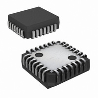
IC REAL TIME CLOCK (RTC) 28-PLCC
Manufacturer
National Semiconductor
Type
Clock/Calendar/NVSRAMr
Datasheet
1.DP8573AVXNOPB.pdf
(16 pages)
Specifications of DP8573AVX/NOPB
Memory Size
32B
Time Format
HH:MM:SS:hh (12/24 hr)
Date Format
YY-MM-DD-dd
Interface
Parallel
Voltage - Supply
4.5 V ~ 5.5 V
Operating Temperature
-40°C ~ 85°C
Mounting Type
Surface Mount
Package / Case
28-PLCC
Bus Type
Parallel
Operating Supply Voltage (typ)
5V
Package Type
PLCC
Operating Supply Voltage (max)
5.5V
Operating Supply Voltage (min)
4.5V
Operating Temperature Classification
Industrial
Operating Temperature (max)
85C
Operating Temperature (min)
-40C
Pin Count
28
Mounting
Surface Mount
Lead Free Status / RoHS Status
Lead free / RoHS Compliant
Other names
*DP8573AVX
*DP8573AVX/NOPB
DP8573AVX
*DP8573AVX/NOPB
DP8573AVX
Available stocks
Company
Part Number
Manufacturer
Quantity
Price
Company:

Part Number:
DP8573AVX/NOPB
Manufacturer:
Texas Instruments
Quantity:
10 000


Functional Description
READING THE CLOCK VALIDATED READ
Since clocking of the counter occurs asynchronously to
reading of the counter it is possible to read the counter
while it is being incremented (rollover) This may result in an
incorrect time reading Thus to ensure a correct reading of
the entire contents of the clock (or that part of interest) it
must be read without a clock rollover occurring In general
this can be done by checking a rollover bit On this chip the
periodic interrupt status bits can serve this function The
following program steps can be used to accomplish this
1 Initialize program for reading clock
2 Dummy read of periodic status bit to clear it
3 Read counter bytes and store
4 Read rollover bit and test it
5 If rollover occured go to 3
6 If no rollover done
To detect the rollover individual periodic status bits can be
polled The periodic bit chosen should be equal to the high-
est frequency counter register to be read That is if only
SECONDS through HOURS counters are read then the
SECONDS periodic bit should be used
READING THE CLOCK INTERRUPT DRIVEN
Enabling the periodic interrupt mask bits cause interrupts
just as the clock rolls over Enabling the desired update rate
and providing an interrupt service routine that executes in
less than 10 ms enables clock reading without checking for
a rollover
READING THE CLOCK LATCHED READ
Another method to read the clock that does not require
checking the rollover bit is to write a one into the Time Save
Enable bit (D7) of the Time Save Control Register and then
to write a zero Writing a one into this bit will enable the
clock contents to be duplicated in the Time Save RAM
Changing the bit from a one to a zero will freeze and store
the contents of the clock in Time Save RAM The time then
can be read without concern for clock rollover since inter-
nal logic takes care of synchronization of the clock Be-
cause only the bits used by the clock counters will be
latched the Time Save RAM should be cleared prior to use
to ensure that random data stored in the unused bits do not
confuse the host microprocessor This bit can also provide
time save at power failure see the Additional Supply Man-
agement Functions section With the Time Save Enable bit
at a logical 0 the Time Save RAM may be used as RAM if
the latched read function is not necessary
INITIALIZING AND WRITING TO THE
CALENDAR-CLOCK
Upon initial application of power to the TCP or when making
time corrections the time must be written into the clock To
correctly write the time to the counters the clock would
normally be stopped by writing the Start Stop bit in the Real
Time Mode Register to a zero This stops the clock from
counting and disables the carry circuitry When initializing
the clock’s Real Time Mode Register it is recommended
that first the various mode bits be written while maintaining
the Start Stop bit reset and then writing to the register a
second time with the Start Stop bit set
(Continued)
6
The above method is useful when the entire clock is being
corrected If one location is being updated the clock need
not be stopped since this will reset the prescaler and time
will be lost An ideal example of this is correcting the hours
for daylight savings time To write to the clock ‘‘on the fly’’
the best method is to wait for the 1 100 of a second period-
ic interrupt Then wait an additional 16
the data to the clock
PRESCALER OSCILLATOR FUNCTIONAL
DESCRIPTION
Feeding the counter chain is a programmable prescaler
which divides the crystal oscillator frequency to 32 kHz and
further to 100 Hz for the counter chain (see Figure 3 )
In addition to the inverter the oscillator feedback bias resis-
tor is included on chip as shown in Figure 4 The oscillator
input may be driven from an external source if desired Re-
fer to test mode application note for details The oscillator
stability is enhanced through the use of an on chip regulated
power supply
The typical range of trimmer capacitor (as shown in Oscilla-
tor Circuit Diagram Figure 4 and in the typical application) at
the oscillator input pin is suggested only to allow accurate
tuning of the oscillator This range is based on a typical
printed circuit board layout and may have to be changed
depending on the parasitic capacitance of the printed circuit
board or fixture being used In all cases the load capaci-
tance specified by the crystal manufacturer (nominal value
11 pF for the 32 768 crystal) is what determines proper os-
cillation This load capcitance is the series combination of
capacitance on each side of the crystal (with respect to
ground)
FIGURE 3 Programmable Clock Prescaler Block
FIGURE 4 Oscillator Circuit Diagram
s and then write
TL F 9981– 8
TL F 9981– 9
Related parts for DP8573AVX/NOPB
Image
Part Number
Description
Manufacturer
Datasheet
Request
R

Part Number:
Description:
IC REAL TIME CLOCK (RTC) 28-PLCC
Manufacturer:
National Semiconductor
Datasheet:

Part Number:
Description:
Clock IC
Manufacturer:
National Semiconductor
Datasheet:

Part Number:
Description:
National Semiconductor [8-Bit D/A Converter]
Manufacturer:
National Semiconductor
Datasheet:
Part Number:
Description:
National Semiconductor [Media Coprocessor]
Manufacturer:
National Semiconductor
Datasheet:
Part Number:
Description:
Digitally Controlled Tone and Volume Circuit with Stereo Audio Power Amplifier, Microphone Preamp Stage and National 3D Sound
Manufacturer:
National Semiconductor
Datasheet:
Part Number:
Description:
Digitally Controlled Tone and Volume Circuit with Stereo Audio Power Amplifier, Microphone Preamp Stage and National 3D Sound
Manufacturer:
National Semiconductor
Datasheet:
Part Number:
Description:
AC97 Rev 2 Codec with Sample Rate Conversion and National 3D Sound
Manufacturer:
National Semiconductor
Part Number:
Description:
Manufacturer:
National Semiconductor
Datasheet:
Part Number:
Description:
Manufacturer:
National Semiconductor
Datasheet:
Part Number:
Description:
General Purpose, Low Voltage, Low Power, Rail-to-Rail Output Operational Amplifiers
Manufacturer:
National Semiconductor
Datasheet:
Part Number:
Description:
8-bit 20 MSPS flash A/D converter.
Manufacturer:
National Semiconductor
Datasheet:
Part Number:
Description:
Low Noise Quad Operational Amplifier
Manufacturer:
National Semiconductor
Datasheet:
Part Number:
Description:
Quad Differential Line Receivers
Manufacturer:
National Semiconductor
Datasheet: