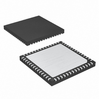
MAX19710ETN+ Maxim Integrated Products, MAX19710ETN+ Datasheet - Page 25

MAX19710ETN+
Manufacturer Part Number
MAX19710ETN+
Description
IC ANLG FRONT END 7.5MSPS 56TQFN
Manufacturer
Maxim Integrated Products
Datasheet
1.MAX19710ETN.pdf
(37 pages)
Specifications of MAX19710ETN+
Number Of Bits
10
Number Of Channels
2
Power (watts)
30mW
Voltage - Supply, Analog
3V
Voltage - Supply, Digital
3V
Package / Case
56-TQFN Exposed Pad
Lead Free Status / RoHS Status
Lead free / RoHS Compliant
= 0, W1 = 0, and W0 = 0. If this value is inadvertently
written to the device, it is ignored and the register con-
tinues to store its previous value. Upon wake-up, the
MAX19710 enters the power mode determined by the
WAKEUP-SEL register, however, all other settings (Tx
DAC offset, Tx DAC common-mode voltage, aux-DAC
settings, aux-ADC state) are restored to their values
prior to shutdown.
The only SPI line that is monitored by the MAX19710
during shutdown is CS/WAKE. Any information transmit-
ted to the MAX19710 concurrent with the CS/WAKE
wake-up pulse is ignored.
The serial digital interface is a standard 3-wire connection
CS/WAKE, SCLK, DIN) compatible with SPI/QSPI™/
MICROWIRE/DSP interfaces. Set CS/WAKE low to enable
the serial data loading at DIN or output at DOUT. Following
a CS/WAKE high-to-low transition, data is shifted synchro-
nously, most significant bit first, on the rising edge of the
Figure 6. Serial-Interface Timing Diagram
Figure 7. Mode-Recovery Timing Diagram
CS/WAKE
CS/WAKE
SCLK
DIN
SCLK
AD0–AD9
DIN
ID/QD
______________________________________________________________________________________
______________________________________________________________________________________
t
CSS
t
DS
MSB
t
DH
t
CH
SPI Timing
t
CP
10-Bit, 7.5Msps, Full-Duplex
t
CL
serial clock (SCLK). After 16 bits are loaded into the serial
input register, data is transferred to the latch when
CS/WAKE transitions high. CS/WAKE must transition high
for a minimum of 80ns before the next write sequence.
SCLK can idle either high or low between transitions.
Figure 6 shows the detailed timing diagram of the 3-wire
serial interface.
Figure 7 shows the mode-recovery timing diagram.
t
or standby mode and entering Rx, Tx, or FD mode.
t
either Rx or Tx mode. t
the Rx ADC to settle within 1dB of specified SINAD per-
formance and Tx DAC settling to 10 LSB error. t
and t
command is latched into the MAX19710 by a CS/WAKE
transition high. In FAST mode, the recovery time is 0.1µs
to switch between Tx or Rx modes.
QSPI is a trademark of Motorola, Inc.
WAKE
ENABLE
LSB
ENABLE
is the wake-up time when exiting shutdown, idle,
is the recovery time when switching between
16-BIT SERIAL DATA INPUT
times are measured after the 16-bit serial
Analog Front-End
t
CS
WAKE
Mode-Recovery Timing
or t
t
t
ADC DIGITAL OUTPUT SINAD
SETTLES TO WITHIN 1dB
DAC ANALOG OUTPUT
SETTLES TO 10 LSB ERROR
WAKE,SD,ST_
WAKE,SD,ST_
ENABLE
t
CSW
TO Rx MODE OR t
TO Tx MODE OR t
is the time for
ENABLE
ENABLE
,
,
WAKE
TX
RX
25
25


