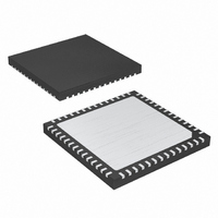
MAX19710ETN+ Maxim Integrated Products, MAX19710ETN+ Datasheet - Page 27

MAX19710ETN+
Manufacturer Part Number
MAX19710ETN+
Description
IC ANLG FRONT END 7.5MSPS 56TQFN
Manufacturer
Maxim Integrated Products
Datasheet
1.MAX19710ETN.pdf
(37 pages)
Specifications of MAX19710ETN+
Number Of Bits
10
Number Of Channels
2
Power (watts)
30mW
Voltage - Supply, Analog
3V
Voltage - Supply, Digital
3V
Package / Case
56-TQFN Exposed Pad
Lead Free Status / RoHS Status
Lead free / RoHS Compliant
Table 12. Auxiliary ADC Convert
Table 15. Auxiliary ADC Averaging
X = Don’t care.
clock by the appropriate divisor (set with bits AD7,
AD8, and AD9; see Table 16) and provides the conver-
sion clock to the auxiliary ADC. The auxiliary ADC has a
maximum conversion rate of 333ksps. The maximum
conversion clock frequency is 4MHz (333ksps x 12
clocks). Choose the proper divider value to keep the
conversion clock frequency under 4MHz, based upon
the system CLK frequency supplied to the MAX19710
(see Table 16). The total conversion time (t
auxiliary ADC can be calculated as t
N
averages (see Table 15), N
Table 16), and f
Table 13. Auxiliary ADC Reference
Table 14. Auxiliary ADC Input Source
AD6
AVG
0
0
0
0
1
1
1
AD3
0
0
1
1
x N
AD0
AD1
AD5
0
1
0
1
0
0
1
1
0
0
1
DIV
) / f
AD4
AD2
CLK
0
1
0
1
0
1
X
0
1
0
1
CLK
______________________________________________________________________________________
______________________________________________________________________________________
is the system CLK frequency.
1 Conversion (No Averaging) (Default)
Internal 2.048V Reference (Default)
; where N
Average of 16 Conversions
Average of 32 Conversions
Average of 32 Conversions
Aux-ADC Start-Convert
Average of 2 Conversions
Average of 4 Conversions
Average of 8 Conversions
Aux-ADC Idle (Default)
Internal V
Aux-ADC INPUT SOURCE
Aux-ADC AVERAGING
DIV
SELECTION
SELECTION
is the CLK divisor (see
AVG
ADC1 (Default)
DD
OV
V
ADC2
DD
is the number of
Reference
DD
/ 2
CONV
/ 2
CONV
= (12 x
) of the
10-Bit, 7.5Msps, Full-Duplex
DOUT is normally in a high-impedance condition. Upon
setting the auxiliary ADC start conversion bit (bit AD0),
DOUT becomes active and goes high, indicating that
the aux-ADC is busy. When the conversion cycle is
complete (including averaging), the data is placed into
an output register and DOUT goes low, indicating that
the output data is ready to be driven onto DOUT. When
bit AD10 is set (AD10 = 1), the aux-ADC enters a data
output mode where data is available at DOUT on the
next low assertion of CS/WAKE. The auxiliary ADC data
is shifted out of DOUT (MSB first) with the data transi-
tioning on the falling edge of the serial clock (SCLK).
Since a DOUT read requires 16 bits, DOUT holds the
value of the last conversion data bit for the last 6 bits (6
least significant bits) following the aux-ADC conversion
data. DOUT enters a high-impedance state when
CS/WAKE is deasserted high. When bit AD10 is cleared
(AD10 = 0), the aux-ADC data is not available on DOUT
(see Table 17).
After the aux-ADC completes a conversion, the data
result is loaded to an output register waiting to be shift-
ed out. No further conversions are possible until data is
shifted out. This means that if the first conversion com-
mand sets AD10 = 0, AD0 = 1, then it cannot be fol-
lowed by conversion commands setting AD10 = 0, AD0
= 1 or AD10 = 1, AD0 = 1. If this sequence of com-
mands is inadvertently used then DOUT is disabled. To
resume normal operation set AD0 = 0.
Table 16. Auxiliary ADC Clock (CLK)
Divider
Table 17. Auxiliary ADC Data Output
Mode
AD9
AD10
0
0
0
0
1
1
1
1
0
1
AD8
0
0
1
1
0
0
1
1
Aux-ADC Data is Not Available on DOUT (Default)
Reading DOUT from the Aux-ADC
Analog Front-End
Aux-ADC Enters Data Output Mode Where
AD7
0
1
0
1
0
1
0
1
Data is Available on DOUT
Aux-ADC CONVERSION CLOCK
CLK Divided by 1 (Default)
SELECTION
CLK Divided by 128
CLK Divided by 16
CLK Divided by 32
CLK Divided by 64
CLK Divided by 2
CLK Divided by 4
CLK Divided by 8
27
27


