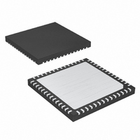
MAX19710ETN+T Maxim Integrated Products, MAX19710ETN+T Datasheet - Page 15

MAX19710ETN+T
Manufacturer Part Number
MAX19710ETN+T
Description
IC ANLG FRNT END 56-TQFN
Manufacturer
Maxim Integrated Products
Datasheet
1.MAX19710ETN.pdf
(37 pages)
Specifications of MAX19710ETN+T
Number Of Bits
10
Number Of Channels
2
Power (watts)
30mW
Voltage - Supply, Analog
3V
Voltage - Supply, Digital
3V
Package / Case
56-TQFN Exposed Pad
Lead Free Status / RoHS Status
Lead free / RoHS Compliant
The MAX19710 integrates a dual, 10-bit Rx ADC and a
dual, 10-bit Tx DAC while providing ultra-low power
and high dynamic performance at 7.5Msps conversion
rate. The Rx ADC analog input amplifiers are fully differ-
5, 7, 12, 40, 50
2, 8, 11, 39,
41, 47, 51
13–22
25–34
PIN
10
23
24
35
36
37
38
42
43
44
45
46
48
49
52
53
54
55
56
—
1
3
4
6
9
CS/WAKE
AD0–AD9
DA0–DA9
OGND
______________________________________________________________________________________
NAME
DOUT
REFIN
OV
ADC2
ADC1
DAC3
DAC2
DAC1
REFP
SCLK
REFN
COM
GND
QAN
QDN
QAP
QDP
CLK
V
IAN
DIN
IDN
IDP
IAP
EP
DD
DD
Detailed Description
Positive Reference Voltage Input Terminal. Bypass with a 0.33µF capacitor to GND as close to REFP
as possible.
Analog Supply Voltage. Bypass V
a 0.1µF capacitor.
Channel-IA Positive Analog Input. For single-ended operation, connect signal source to IAP.
Channel-IA Negative Analog Input. For single-ended operation, connect IAN to COM.
Analog Ground. Connect all GND pins to ground plane.
Conversion Clock Input. Clock signal for both receive ADCs and transmit DACs.
Channel-QA Negative Analog Input. For single-ended operation, connect QAN to COM.
Channel-QA Positive Analog Input. For single-ended operation, connect signal source to QAP.
Receive ADC Digital Outputs. AD9 is the most significant bit (MSB) and AD0 is the least significant
bit (LSB).
Output-Driver Ground
Output-Driver Power Supply. Supply range from +1.8V to V
combination of a 2.2µF capacitor in parallel with a 0.1µF capacitor.
Transmit DAC Digital Inputs. DA9 is the most significant bit (MSB) and DA0 is the least significant bit
(LSB). DA0–DA9 are internally pulled up to OV
Aux-ADC Digital Output
3-Wire Serial-Interface Data Input. Data is latched on the rising edge of SCLK.
3-Wire Serial-Interface Clock Input
3-Wire Serial-Interface Chip-Select/WAKE Input. When the MAX19710 is in shutdown, CS/WAKE
controls the wake-up function. See the Wake-Up Function section.
Selectable Auxiliary ADC Analog Input 2
Selectable Auxiliary ADC Analog Input 1
Auxiliary DAC3 Analog Output (V
Auxiliary DAC2 Analog Output (V
Auxiliary DAC1 Analog Output (AFC DAC, V
Tx Path Channel-ID Differential Negative Output
Tx Path Channel-ID Differential Positive Output
Tx Path Channel-QD Differential Negative Output
Tx Path Channel-QD Differential Positive Output
Reference Input. Connect to V
Common-Mode Voltage I/O. Bypass COM to GND with a 0.33µF capacitor.
Negative Reference Voltage Input Terminal. Rx ADC conversion range is ±(V
REFN to GND with a 0.33µF capacitor.
Exposed Paddle. Exposed paddle is internally connected to GND. Connect EP to the GND plane.
10-Bit, 7.5Msps, Full-Duplex
DD
OUT
OUT
DD
for internal reference.
to GND with a combination of a 2.2µF capacitor in parallel with
= 0 at Power-Up)
= 0 at Power-Up)
ential and accept 1.024V
DAC analog outputs are fully differential with ±400mV
full-scale output, selectable common-mode DC level,
and adjustable channel ID–QD offset trim.
OUT
FUNCTION
DD.
= 1.1V at Power-Up)
Analog Front-End
DD
. Bypass OV
P-P
full-scale signals. The Tx
Pin Description
DD
REFP
to OGND with a
- V
REFN
). Bypass
15


