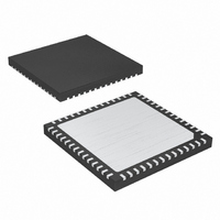
MAX19710ETN+T Maxim Integrated Products, MAX19710ETN+T Datasheet - Page 6

MAX19710ETN+T
Manufacturer Part Number
MAX19710ETN+T
Description
IC ANLG FRNT END 56-TQFN
Manufacturer
Maxim Integrated Products
Datasheet
1.MAX19710ETN.pdf
(37 pages)
Specifications of MAX19710ETN+T
Number Of Bits
10
Number Of Channels
2
Power (watts)
30mW
Voltage - Supply, Analog
3V
Voltage - Supply, Digital
3V
Package / Case
56-TQFN Exposed Pad
Lead Free Status / RoHS Status
Lead free / RoHS Compliant
ELECTRICAL CHARACTERISTICS (continued)
(V
amplitude = -0.5dBFS, Tx DAC output amplitude = 0dBFS, CM1 = 0, CM0 = 0, differential Rx ADC input, differential Tx DAC output,
C
T
10-Bit, 7.5Msps, Full-Duplex
Analog Front-End
6
Full-Scale Reference
Analog Input Range
Analog Input Impedance
Input-Leakage Current
Gain Error
Zero-Code Error
Differential Nonlinearity
Integral Nonlinearity
Supply Current
AUXILIARY DACs (DAC1, DAC2, DAC3)
Resolution
Integral Nonlinearity
Differential Nonlinearity
Output-Voltage Low
Output-Voltage High
DC Output Impedance
Settling Time
Glitch Impulse
Rx ADC–Tx DAC TIMING CHARACTERISTICS
CLK Rise to Channel-I Output Data
Valid
CLK Fall to Channel-Q Output
Data Valid
I-DAC DATA to CLK Fall Setup
Time
Q-DAC DATA to CLK Rise Setup
Time
CLK Fall to I-DAC Data Hold Time
CLK Rise to Q-DAC Data Hold
Time
CLK Duty Cycle
CLK Duty-Cycle Variation
Digital Output Rise/Fall Time
A
REFP
DD
= +25°C.) (Note 1)
_______________________________________________________________________________________
= 3V, OV
= C
REFN
PARAMETER
DD
= C
= 1.8V, internal reference (1.024V), C
COM
= 0.33µF, C
L
< 5pF on all aux-DAC outputs, T
SYMBOL
V
t
t
t
DNL
DNL
V
V
t
t
DOQ
t
DHQ
INL
INL
DSQ
GE
ZE
DOI
DHI
DSI
REF
N
OH
OL
AD1 = 0 (default)
AD1 = 1
Measured at DC
Measured at unselected input from 0 to
V
Includes reference error, AD1 = 0
From code 100 to code 4000
Guaranteed monotonic over code 100 to
code 4000 (Note 2)
R
R
DC output at midscale
From code 1024 to code 3072, within ±10
LSB
From code 0 to code 4095
Figure 3 (Note 2)
Figure 3 (Note 2)
Figure 5 (Note 2)
Figure 5 (Note 2)
Figure 5 (Note 2)
Figure 5 (Note 2)
20% to 80%
REF
L
L
> 200kΩ
> 200kΩ
L
≈ 10pF on all digital outputs, f
CONDITIONS
A
= T
MIN
to T
MAX
CLK
, unless otherwise noted. Typical values are at
= 7.5MHz (50% duty cycle), Rx ADC input
2.57
MIN
-1.0
5.5
6.5
12
10
10
-5
0
0
±1.25
±0.65
2.048
V
±0.1
±0.6
±0.6
TYP
V
±15
0 to
500
210
8.2
9.3
2.4
±2
24
50
REF
DD
4
1
MAX
+1.2
11.5
13.0
0.2
+5
UNITS
%FS
nV
LSB
LSB
LSB
LSB
Bits
mV
kΩ
µA
µA
µs
ns
ns
ns
ns
ns
ns
ns
%
%
Ω
V
V
V
V
•
s


