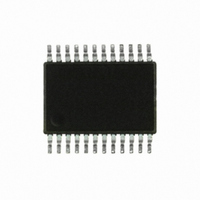
CS5550-ISZ Cirrus Logic Inc, CS5550-ISZ Datasheet - Page 18

CS5550-ISZ
Manufacturer Part Number
CS5550-ISZ
Description
IC ADC 2CH LOW-COST 24SSOP
Manufacturer
Cirrus Logic Inc
Datasheet
1.CS5550-ISZ.pdf
(24 pages)
Specifications of CS5550-ISZ
Number Of Converters
2
Package / Case
24-SSOP
Number Of Bits
2
Sampling Rate (per Second)
4k
Data Interface
Serial
Power Dissipation (max)
30mW
Voltage Supply Source
Analog and Digital
Operating Temperature
-40°C ~ 85°C
Mounting Type
Surface Mount
Number Of Adc Inputs
2
Architecture
Delta-Sigma
Conversion Rate
4 KSPs
Resolution
24 bit
Input Type
Voltage
Interface Type
Serial (3-Wire)
Voltage Reference
2.5 V
Supply Voltage (max)
5 V
Supply Voltage (min)
3.3 V
Maximum Operating Temperature
+ 85 C
Mounting Style
SMD/SMT
Input Voltage
3.3 V to 5 V
Minimum Operating Temperature
- 40 C
Lead Free Status / RoHS Status
Lead free / RoHS Compliant
Lead Free Status / RoHS Status
Lead free / RoHS Compliant, Lead free / RoHS Compliant
Other names
598-1119-5
Available stocks
Company
Part Number
Manufacturer
Quantity
Price
Part Number:
CS5550-ISZ
Manufacturer:
CIRRUS
Quantity:
20 000
4.2 Serial Port Interface
The CS5550’s serial interface consists of four con-
trol lines, which have the following pin-names: CS,
SDI, SDO, and SCLK.
CS, Chip Select, is the control line which enables
access to the serial port. If the CS pin is tied to logic
0, the port can function as a three wire interface.
SDI, Serial Data In, is the data signal used to trans-
fer data to the converters.
SDO, Serial Data Out, is the data signal used to
transfer output data from the converters. The SDO
output will be held at high impedance any time CS
is at logic 1.
SCLK, Serial Clock, is the serial bit-clock which
controls the shifting of data to or from the ADC’s
serial port. The CS pin must be held at logic 0 be-
fore SCLK transitions can be recognized by the
port logic. To accommodate opto-isolators SCLK is
designed with a Schmitt-trigger input to allow an
opto-isolator with slower rise and fall times to di-
rectly drive the pin. Additionally, SDO is capable of
sinking or sourcing up to 5 mA to directly drive an
opto-isolator LED. SDO will have less than a
400 mV loss in the drive voltage when sinking or
sourcing 5 mA.
4.3 Serial Read and Write
The state machine decodes the command word as
it is received. Data is written to and read from the
CS5550 by using the Register Read/Write com-
mand. Figure 1 illustrates the serial sequence nec-
essary to write to, or read from the serial port’s
buffers. As shown in Figure 1, a transfer of data is
always initiated by sending the appropriate 8-bit
command (MSB first) to the serial port (SDI pin).
4.3.1 Register Write
When a command involves a write operation, the
serial port will continue to clock in the data bits
(MSB first) on the SDI pin for the next 24 SCLK cy-
cles. Command words instructing a register write
must be followed by 24 bits of data. To write the
Configuration Register, the user would transmit the
command (0x40) to initiate a write to the Configu-
ration Register. The CS5550 will then acquire the
serial data input from the (SDI) pin when the user
pulses the serial clock (SCLK) 24 times. Once the
18
data is received, the state machine writes the data
to the Configuration Register and then waits to re-
ceive another valid command.
4.3.2 Register Read
When a read command is initiated, the serial port
will start transferring register content bits serial
(MSB first) on the SDO pin for the next 8, 16, or 24
SCLK cycles. Command words instructing a regis-
ter read may be terminated at 8-bit boundaries
(e.g., read transfers may be 8, 16, or 24 bits in
length). Also data register reads allow “command
chaining”. This means that the micro-controller is
allowed to send a new command while reading
register data. The new command will be acted
upon immediately and could possibly terminate the
first register read. For example, if the user is only
interested in acquiring the 16 most significant bits
of data from the first read, then the user can begin
to strobe a second read command on SDI after the
first 8 data bits have been read from SDO.
During the read cycle, the SYNC0 command
(NOP) should be strobed on the SDI port while
clocking the data from the SDO port.
4.4 System Initialization
A software or hardware reset can be initiated at
any time. The software reset is initiated by sending
the command 0x80.
A hardware reset is initiated when the RESET pin
is forced low with a minimum pulse width of 50 ns.
The RESET signal is asynchronous, requiring no
MCLKs for the part to detect and store a reset
event. The RESET pin is a Schmitt Trigger input,
which allows it to accept slow rise times and/or
noisy control signals. Once the RESET pin is inac-
tive, the internal reset circuitry remains active for 5
MCLK cycles to insure resetting the synchronous
circuitry in the device. The modulators are held in
reset for 12 MCLK cycles after RESET becomes
inactive. After a hardware or software reset, the in-
ternal registers (some of which drive output pins)
will be reset to their default values on the first MCLK
received after detecting a reset event. The internal
register values are also set to their default values af-
ter initial power-on of the device. The CS5550 will
then assume its active state. (The term active state,
CS5550
DS630F1


