CS5550-ISZ Cirrus Logic Inc, CS5550-ISZ Datasheet - Page 4
CS5550-ISZ
Manufacturer Part Number
CS5550-ISZ
Description
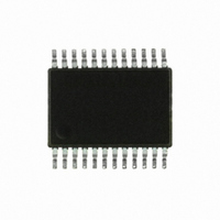
IC ADC 2CH LOW-COST 24SSOP
Manufacturer
Cirrus Logic Inc
Datasheet
1.CS5550-ISZ.pdf
(24 pages)
Specifications of CS5550-ISZ
Number Of Converters
2
Package / Case
24-SSOP
Number Of Bits
2
Sampling Rate (per Second)
4k
Data Interface
Serial
Power Dissipation (max)
30mW
Voltage Supply Source
Analog and Digital
Operating Temperature
-40°C ~ 85°C
Mounting Type
Surface Mount
Number Of Adc Inputs
2
Architecture
Delta-Sigma
Conversion Rate
4 KSPs
Resolution
24 bit
Input Type
Voltage
Interface Type
Serial (3-Wire)
Voltage Reference
2.5 V
Supply Voltage (max)
5 V
Supply Voltage (min)
3.3 V
Maximum Operating Temperature
+ 85 C
Mounting Style
SMD/SMT
Input Voltage
3.3 V to 5 V
Minimum Operating Temperature
- 40 C
Lead Free Status / RoHS Status
Lead free / RoHS Compliant
Lead Free Status / RoHS Status
Lead free / RoHS Compliant, Lead free / RoHS Compliant
Other names
598-1119-5
Available stocks
Company
Part Number
Manufacturer
Quantity
Price

Part Number:
CS5550-ISZ
Manufacturer:
CIRRUS
Quantity:
20 000


1. PIN DESCRIPTION
4
Clock Generator
Crystal Out
Crystal In
CPU Clock Output
Control Pins and Serial Data I/O
Serial Clock Input
Serial Data Output
Chip Select
Reset
Interrupt
Serial Data Input
Measurement and Reference Input
Differential
Analog Inputs
Voltage
Reference Output
Voltage
Reference Input
Power Supply Connections
Positive
Digital Supply
Digital Ground
Positive
Analog Supply
Analog Ground
Test Output
Voltage Reference Output
Voltage Reference Input
Differential Analog Input
Differential Analog Input
Positive Power Supply
CPU Clock Output
Serial Data Ouput
8,17,18,21,22 TSTO - These pins are used for factory testing and must be left floating.
9,10,15,16
Digital Ground
4,9,10
Serial Clock
1,24
Test Output
Chip Select
Crystal Out
19
20
23
12
14
1
11
2
5
6
7
3
3
XOUT, XIN - A gate inside the chip is connected to these pins and can be used with a
crystal to provide the system clock for the device. Alternatively, an external (CMOS
compatible) clock can be supplied into XIN pin to provide the system clock for the device.
CPUCLK - Output of on-chip oscillator which can drive one standard CMOS load.
SCLK - A clock signal on this pin determines the input and output rate of the data for the
SDI and SDO pins respectively. The SCLK pin will recognize clocks only when CS is low.
SDO -The serial data port output pin. Its output is in a high impedance state when CS is
high.
CS - When low, the port will recognize SCLK. An active high on this pin forces the SDO
pin to a high impedance state. CS should be changed when SCLK is low.
RESET - When reset is taken low, all internal registers are set to their default states.
INT - When INT goes low it signals that an enabled event has occurred.
SDI - The serial data port input pin. Data will be input at a rate determined by SCLK.
AIN1+, AIN1-, AIN2+, AIN2- - Differential analog input pins.
VREFOUT - The on-chip voltage reference output. The voltage reference has a nominal
magnitude of 2.5 V and is referenced to the AGND pin on the converter.
VREFIN - The input establishes the voltage reference for the on-chip modulator.
VD+ - The positive digital supply relative to DGND.
DGND - The common-mode potential of digital ground must be equal to or above the
common-mode potential of AGND.
VA+ - The positive analog supply relative to AGND.
AGND - The analog ground pin must be at the lowest potential.
VREFOUT
CPUCLK
VREFIN
DGND
AIN2+
XOUT
SCLK
TSTO
AIN2-
SDO
VD+
CS
1
2
3
4
5
6
7
8
9
10
11
12
24
23
22
21
20
19
18
17
16
15
14
13
XIN
SDI
TSTO
TSTO
INT
RESET
TSTO
TSTO
AIN1+
AIN1-
VA+
AGND
Crystal In
Serial Data Input
Test Output
Test Output
Interrupt
Reset
Test Output
Test Output
Differential Analog Input
Differential Analog Input
Positive Analog Supply
Analog Ground
CS5550
DS630F1
Related parts for CS5550-ISZ
Image
Part Number
Description
Manufacturer
Datasheet
Request
R

Part Number:
Description:
IC,A/D CONVERTER,DUAL,24-BIT,SSOP,24PIN
Manufacturer:
Cirrus Logic Inc
Datasheet:


Part Number:
Description:
Development Kit
Manufacturer:
Cirrus Logic Inc
Datasheet:
Part Number:
Description:
Development Kit
Manufacturer:
Cirrus Logic Inc
Datasheet:


Part Number:
Description:
High-efficiency PFC + Fluorescent Lamp Driver Reference Design
Manufacturer:
Cirrus Logic Inc
Datasheet:
Part Number:
Description:
Development Kit
Manufacturer:
Cirrus Logic Inc
Datasheet:
Part Number:
Description:
Development Kit
Manufacturer:
Cirrus Logic Inc
Datasheet:

Part Number:
Description:
Development Kit
Manufacturer:
Cirrus Logic Inc
Datasheet:
Part Number:
Description:
Development Kit
Manufacturer:
Cirrus Logic Inc
Datasheet:
Part Number:
Description:
Development Kit
Manufacturer:
Cirrus Logic Inc
Datasheet:
Part Number:
Description:
Development Kit
Manufacturer:
Cirrus Logic Inc
Datasheet:

Part Number:
Description:
Ref Bd For Speakerbar MSA & DSP Products
Manufacturer:
Cirrus Logic Inc