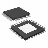
AD7760BSVZ Analog Devices Inc, AD7760BSVZ Datasheet - Page 20

AD7760BSVZ
Manufacturer Part Number
AD7760BSVZ
Description
IC ADC 24BIT 2.5MSPS 64TQFP
Manufacturer
Analog Devices Inc
Datasheet
1.AD7760BSVZ.pdf
(36 pages)
Specifications of AD7760BSVZ
Data Interface
Parallel
Number Of Bits
24
Sampling Rate (per Second)
2.5M
Number Of Converters
1
Power Dissipation (max)
958mW
Voltage Supply Source
Analog and Digital
Operating Temperature
-40°C ~ 85°C
Mounting Type
Surface Mount
Package / Case
64-TQFP Exposed Pad
Resolution (bits)
24bit
Sampling Rate
2.5MSPS
Input Channel Type
Differential
Supply Voltage Range - Digital
2.375V To 2.625V
Supply Current
49mA
Lead Free Status / RoHS Status
Lead free / RoHS Compliant
Available stocks
Company
Part Number
Manufacturer
Quantity
Price
Company:
Part Number:
AD7760BSVZ
Manufacturer:
Analog Devices Inc
Quantity:
10 000
Part Number:
AD7760BSVZ
Manufacturer:
ADI/亚德诺
Quantity:
20 000
Company:
Part Number:
AD7760BSVZ-REEL
Manufacturer:
Analog Devices Inc
Quantity:
10 000
AD7760
MODULATOR DATA OUTPUT MODE INTERFACE
The AD7760 can be configured in modulator data output mode
(bypassing the default decimation filtering) by writing 0 to each
of the bits contained in Control Register 1: BYP F1 , BYP F3 ,
and DEC [2:0]. This will bypass all digital decimation filtering
offered by the AD7760. See the AD7760 Registers section for
further details.
When the AD7760 is operating in modulator data output mode,
a different parallel interfacing scheme than that used for config-
urations, where the AD7760’s data output is filtered is necessary.
The data output rate depends on the clock divider ratio that is
used. When the CDIV bit in Control Register 2 is set to logic
high, data is output at the MCLK frequency. If the CDIV bit is
set to logic low, data is output at a frequency of MCLK/2. See
the Clocking the AD7760 section.
CLOCK DIVIDE-BY-1 MODE (CDIV = 1)
When obtaining data from the AD7760 in modulator output
mode, both the RD /WR and CS lines must be held low. This
brings the data bus out of its high impedance state. Figure 43
shows the timing diagram for reading data in the modulator data
RESET
MCLK
SYNC
CS, RD/WR
D[0:15]
DRDY
Figure 44. AD7760 Relative Timing Between RESET and SYNC in Modulator Output Mode CDIV = 0
t
Figure 43. AD7760 Modulator Output Mode ( CDIV = 1) and ( CDIV = 0, n is even)
11
INVALID DATA
t
9
Rev. A | Page 20 of 36
t
10
MOD DATA M
t
12
t
13
output mode when operating with CDIV = 1 (that is, ICLK =
MCLK). A DRDY pulse is generated for each word. The data on
each of the 16 data output pins, D [15:0], is valid on the rising
edge of the DRDY pulse. The DRDY pulse can be used to latch
the modulator data into a FIFO or as a DMA control signal. Shortly
after the RD /WR and CS lines return high, the AD7760 stops
outputting data and the data bus returns to high impedance.
CLOCK DIVIDE-BY-2 MODE (CDIV = 0)
When operating in modulator output mode with CDIV = 0
(that is, ICLK = MCLK/2), the frequency of the DRDY signal
created is half that of the MCLK frequency input to the device.
The timing scheme that is used when CDIV = 0 depends on the
number of MCLK cycles that occur between RESET and SYNC .
If the number of MCLK cycles (n) between the rising edge of
RESET and the rising edge of SYNC (see Figure 44) is an even
value, use the interface timing shown in Figure 43. If n is an odd
value, use the interface timing shown in Figure 45.
n ×
t
MCLK
MOD DATA M + 1
MOD D...
t
14


