AD7760BSVZ Analog Devices Inc, AD7760BSVZ Datasheet - Page 33
AD7760BSVZ
Manufacturer Part Number
AD7760BSVZ
Description
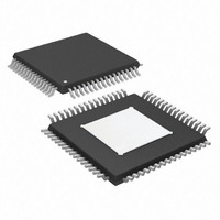
IC ADC 24BIT 2.5MSPS 64TQFP
Manufacturer
Analog Devices Inc
Datasheet
1.AD7760BSVZ.pdf
(36 pages)
Specifications of AD7760BSVZ
Data Interface
Parallel
Number Of Bits
24
Sampling Rate (per Second)
2.5M
Number Of Converters
1
Power Dissipation (max)
958mW
Voltage Supply Source
Analog and Digital
Operating Temperature
-40°C ~ 85°C
Mounting Type
Surface Mount
Package / Case
64-TQFP Exposed Pad
Resolution (bits)
24bit
Sampling Rate
2.5MSPS
Input Channel Type
Differential
Supply Voltage Range - Digital
2.375V To 2.625V
Supply Current
49mA
Lead Free Status / RoHS Status
Lead free / RoHS Compliant
Available stocks
Company
Part Number
Manufacturer
Quantity
Price
Company:

Part Number:
AD7760BSVZ
Manufacturer:
Analog Devices Inc
Quantity:
10 000
Part Number:
AD7760BSVZ
Manufacturer:
ADI/亚德诺
Quantity:
20 000
Company:
Part Number:
AD7760BSVZ-REEL
Manufacturer:
Analog Devices Inc
Quantity:
10 000


AD7760 REGISTERS
The AD7760 has a number of user-programmable registers. The control registers are used to set the decimation rate, the filter configuration, the
clock divider, and so on. There are also digital gain, offset, and overrange threshold registers. Writing to these registers involves writing
the register address first, then a 16-bit data-word. Register addresses, details of individual bits, and default values are given in this section.
CONTROL REGISTER 1—ADDRESS 0x0001
Default Value 0x001A
MSB
D15
DL_
FILT
Table 15. Bit Descriptions of Control Register 1
Bit
15
14
13
12
11
10
9
8 to 5
4
3
2 to 0
1
2
CONTROL REGISTER 2—ADDRESS 0x0002
Default Value After RESET : 0x009B
Recommended register setting for power-up and normal operation using clock divide-by-2 ( CDIV = 0) mode: 0x0002
MSB
D15
0
Table 16. Bit Descriptions of Control Register 2
Bit
5
3
2
1
0
Bit 15 to Bit 9 are self-clearing bits.
Only one of the bits from Bit 14 to Bit 11 can be set in any write operation because it determines the contents of the next read operation.
Mnemonic
CDIV
PD
LPWR
1
D1PD
D14
RD
OVR
D14
0
Mnemonic
DL_FILT
RD OVR
RD GAIN
RD OFF
RD STAT
0
SYNC
FLEN [3:0]
BYP F3
BYP F1
DEC [2:0]
1
D13
RD
GAIN
D13
0
1, 2
1, 2
1
1, 2
1, 2
Description
Clock Divider Bit. This sets the divide ratio of the MCLK signal to produce the internal ICLK. Setting CDIV = 0 divides the
MCLK by 2. If CDIV = 1, the ICLK frequency is equal to the MCLK.
Power Down. Setting this bit powers down the AD7760, reducing the power consumption to 6.35 mW.
Low Power. If this bit is set, the AD7760 is operating in a low power mode. The power consumption is reduced for a 6 dB
reduction in noise performance.
Write 1 to this bit.
Differential Amplifier Power Down. Setting this bit powers down the on-chip differential amplifier.
D12
RD
OFF
D12
0
Description
Download Filter. Before downloading a user-defined filter, this bit must be set. The filter length bits must
also be set at this time. The write operations that follow are interpreted as the user coefficients for the FIR
filter until all the coefficients and the checksum have been written.
Read Overrange. If this bit has been set, the next read operation outputs the contents of the overrange
threshold register instead of a conversion result.
Read Gain. If this bit has been set, the next read operation outputs the contents of the digital gain register.
Read Offset. If this bit has been set, the next read operation outputs the contents of the digital offset register.
Read Status. If this bit has been set, the next read operation outputs the contents of the status register.
0 must be written to this bit.
Synchronize. Setting this bit initiates an internal synchronization routine. Setting this bit simultaneously on
multiple devices synchronizes all filters.
Filter Length Bits. These bits must be set when the DL_FILT bit is set before a user-defined filter is downloaded.
Bypass Filter 3. If this bit is 0, Filter 3 (programmable FIR) is bypassed.
Bypass Filter 1. If this bit is 0, Filter 1 is bypassed. This should only occur when the user requires unfiltered
modulator data to be output.
Decimation Rate. These bits set the decimation rate of Filter 2. All 0s implies that the filter is bypassed. A value
of 1 corresponds to 2× decimation, a value of 2 corresponds to 4× decimation, and so on, up to the maximum
value of 5, corresponding to 32× decimation.
D11
RD
STAT
D11
0
D10
0
D10
0
D9
SYNC
D9
0
D8
FLEN3
D8
0
Rev. A | Page 33 of 36
D7
0
D7
FLEN2
D6
FLEN1
D6
0
D5
CDIV
D5
FLEN0
D4
BYP F3
D4
0
D3
PD
D3
BYP F1
D2
DEC2
D2
LPWR
D1
DEC1
D1
1
AD7760
D0
LSB
D0
D1PD
LSB
DEC0
Related parts for AD7760BSVZ
Image
Part Number
Description
Manufacturer
Datasheet
Request
R

Part Number:
Description:
±1.7g Dual-Axis IMEMS Accelerometer Evaluation Board
Manufacturer:
Analog Devices Inc
Datasheet:

Part Number:
Description:
Inertial Sensor Evaluation System
Manufacturer:
Analog Devices Inc
Datasheet:
Part Number:
Description:
Manufacturer:
Analog Devices Inc
Datasheet:
Part Number:
Description:
Manufacturer:
Analog Devices Inc
Datasheet:
Part Number:
Description:
Manufacturer:
Analog Devices Inc
Datasheet:
Part Number:
Description:
Manufacturer:
Analog Devices Inc
Datasheet:
Part Number:
Description:
Manufacturer:
Analog Devices Inc
Datasheet:
Part Number:
Description:
Manufacturer:
Analog Devices Inc
Datasheet:
Part Number:
Description:
Manufacturer:
Analog Devices Inc
Datasheet:
Part Number:
Description:
Manufacturer:
Analog Devices Inc
Datasheet:
Part Number:
Description:
Manufacturer:
Analog Devices Inc
Datasheet:
Part Number:
Description:
Manufacturer:
Analog Devices Inc
Datasheet:
Part Number:
Description:
Manufacturer:
Analog Devices Inc
Datasheet: