AD7760BSVZ Analog Devices Inc, AD7760BSVZ Datasheet - Page 26
AD7760BSVZ
Manufacturer Part Number
AD7760BSVZ
Description
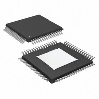
IC ADC 24BIT 2.5MSPS 64TQFP
Manufacturer
Analog Devices Inc
Datasheet
1.AD7760BSVZ.pdf
(36 pages)
Specifications of AD7760BSVZ
Data Interface
Parallel
Number Of Bits
24
Sampling Rate (per Second)
2.5M
Number Of Converters
1
Power Dissipation (max)
958mW
Voltage Supply Source
Analog and Digital
Operating Temperature
-40°C ~ 85°C
Mounting Type
Surface Mount
Package / Case
64-TQFP Exposed Pad
Resolution (bits)
24bit
Sampling Rate
2.5MSPS
Input Channel Type
Differential
Supply Voltage Range - Digital
2.375V To 2.625V
Supply Current
49mA
Lead Free Status / RoHS Status
Lead free / RoHS Compliant
Available stocks
Company
Part Number
Manufacturer
Quantity
Price
Company:

Part Number:
AD7760BSVZ
Manufacturer:
Analog Devices Inc
Quantity:
10 000
Part Number:
AD7760BSVZ
Manufacturer:
ADI/亚德诺
Quantity:
20 000
Company:
Part Number:
AD7760BSVZ-REEL
Manufacturer:
Analog Devices Inc
Quantity:
10 000


AD7760
DRIVING THE AD7760
The AD7760 has an on-chip differential amplifier that operates
with a supply voltage (AV
For a 4.096 V reference, the supply voltage must be 5 V.
To achieve the specified performance in normal mode, the
differential amplifier should be configured as a first-order
antialias filter, as shown in Figure 50. Any additional filtering
should be carried out in previous stages using low noise, high
performance op amps, such as the AD8021.
Suitable component values for the first-order filter are listed in
Table 8. Using the values in the table as an example yields a
10 dB attenuation at the first alias point of 19 MHz.
Table 8. Normal Mode Component Values
V
4.096 V
Figure 52 shows the signal conditioning that occurs using the
circuit shown in Figure 50 with a ±2.5 V input signal biased
around ground and the component values and conditions listed
in Table 8. The differential amplifier always biases the output
REF
R
1 kΩ
IN
Figure 50. Differential Amplifier Configuration
A
B
R
655 Ω
R
R
FB
IN
C
IN
DD
S
INPUTS TO THE AD7760 DIFFERENTIAL AMPLIFIER
3) within the 3.15 V to 5.25 V range.
+2.5V
–2.5V
+2.5V
–2.5V
R
C
0V
0V
C
R
A1
FB
FB
FB
FB
R
18 Ω
M
R
R
M
M
A
B
C
5.6 pF
S
Figure 52. Differential Amplifier Signal Conditioning
V
V
IN
IN
–
+
C
33 pF
FB
Rev. A | Page 26 of 36
OUTPUTS OF THE AD7760 DIFFERENTIAL AMPLIFIER
+3.685V
+2.048V
+0.410V
+3.685V
+2.048V
+0.410V
OUTPUT
signal to sit on the optimum common mode of V
case 2.048 V. The signal is also scaled to give the maximum
allowable voltage swing with this reference value. This is
calculated as 80% of V
on each input.
With a 4.096 V reference, a 5 V supply must be provided to the
reference buffer (AV
must be provided to AV
Figure 51 shows the transfer function in terms of the 24-bit
digital output codes (twos complement coding) of the AD7760
vs. the voltage signals V
differential amplifier A1, as shown in Figure 52.
AD7760
Figure 51. Transfer Function for the AD7760 Filtered Output Where V
24-BIT
011…111
011…110
000…010
000…001
000…000
111…111
111…110
100…001
100…000
24 BITS
are Inputs to the On-Board Differential Amplifier A1
B = +2.5V
A = –2.5V
DD
REF
4). With a 2.5 V reference, a 3.3 V supply
V
V
A
DD
IN
IN
, that is, 0.8 × 4.096 V ≈ 3.275 V p-p
and V
+
–
4.
B
applied to the on-board
A = 0V
B = 0V
REF
/2, in this
A = +2.5V
B = –2.5V
A
and V
B
Related parts for AD7760BSVZ
Image
Part Number
Description
Manufacturer
Datasheet
Request
R

Part Number:
Description:
±1.7g Dual-Axis IMEMS Accelerometer Evaluation Board
Manufacturer:
Analog Devices Inc
Datasheet:

Part Number:
Description:
Inertial Sensor Evaluation System
Manufacturer:
Analog Devices Inc
Datasheet:
Part Number:
Description:
Manufacturer:
Analog Devices Inc
Datasheet:
Part Number:
Description:
Manufacturer:
Analog Devices Inc
Datasheet:
Part Number:
Description:
Manufacturer:
Analog Devices Inc
Datasheet:
Part Number:
Description:
Manufacturer:
Analog Devices Inc
Datasheet:
Part Number:
Description:
Manufacturer:
Analog Devices Inc
Datasheet:
Part Number:
Description:
Manufacturer:
Analog Devices Inc
Datasheet:
Part Number:
Description:
Manufacturer:
Analog Devices Inc
Datasheet:
Part Number:
Description:
Manufacturer:
Analog Devices Inc
Datasheet:
Part Number:
Description:
Manufacturer:
Analog Devices Inc
Datasheet:
Part Number:
Description:
Manufacturer:
Analog Devices Inc
Datasheet:
Part Number:
Description:
Manufacturer:
Analog Devices Inc
Datasheet: