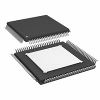
AD9446BSVZ-100 Analog Devices Inc, AD9446BSVZ-100 Datasheet - Page 11

AD9446BSVZ-100
Manufacturer Part Number
AD9446BSVZ-100
Description
IC ADC 16BIT 100MSPS 100-TQFP
Manufacturer
Analog Devices Inc
Datasheet
1.AD9446BSVZ-100.pdf
(36 pages)
Specifications of AD9446BSVZ-100
Data Interface
Parallel
Number Of Bits
16
Sampling Rate (per Second)
100M
Number Of Converters
1
Power Dissipation (max)
2.8W
Voltage Supply Source
Single Supply
Operating Temperature
-40°C ~ 85°C
Mounting Type
Surface Mount
Package / Case
100-TQFP Exposed Pad
Resolution (bits)
16bit
Sampling Rate
100MSPS
Input Channel Type
Differential, Single Ended
Supply Voltage Range - Digital
3V To 3.6V
Supply Current
368mA
Number Of Elements
1
Resolution
16Bit
Architecture
Pipelined
Sample Rate
100MSPS
Input Polarity
Bipolar
Input Type
Voltage
Rated Input Volt
±1/±1.6V
Differential Input
Yes
Power Supply Requirement
Single
Single Supply Voltage (typ)
3.3/5V
Single Supply Voltage (min)
3.14/4.75V
Single Supply Voltage (max)
3.46/5.25V
Dual Supply Voltage (typ)
Not RequiredV
Dual Supply Voltage (min)
Not RequiredV
Dual Supply Voltage (max)
Not RequiredV
Power Dissipation
2.8W
Differential Linearity Error
±0.85LSB
Integral Nonlinearity Error
±6LSB
Operating Temp Range
-40C to 85C
Operating Temperature Classification
Industrial
Mounting
Surface Mount
Pin Count
100
Package Type
TQFP EP
Input Signal Type
Differential
Package
100TQFP EP
Number Of Analog Inputs
1
Digital Interface Type
Parallel
Signal To Noise Ratio
79.7(Typ) dB
Lead Free Status / RoHS Status
Lead free / RoHS Compliant
For Use With
AD9446-80LVDS/PCBZ - BOARD EVALUATION AD9446-80
Lead Free Status / Rohs Status
Compliant
Available stocks
Company
Part Number
Manufacturer
Quantity
Price
Company:
Part Number:
AD9446BSVZ-100
Manufacturer:
AD
Quantity:
138
Company:
Part Number:
AD9446BSVZ-100
Manufacturer:
ADI
Quantity:
132
Part Number:
AD9446BSVZ-100
Manufacturer:
ADI/亚德诺
Quantity:
20 000
Table 7. Pin Function Descriptions—100-Lead TQFP/EP in LVDS Mode
Pin No.
1
2
3
4
5
6, 18 to 20, 32 to 34, 36, 38,
43 to 45, 92 to 97
7
8
9, 21, 24, 39, 42, 46, 91, 98,
99, 100, Exposed Heat Sink
10
11
12 to 17, 25 to 31, 35, 37
22
23
40
41
47, 63, 75, 87,
48, 64, 76, 88
49
50
51
52
53
54
55
56
57
58
59
60
61
62
65
66
67
68
69
70
71
72
73
74
77
78
Mnemonic
DCS MODE
DNC
OUTPUT
MODE
DFS
LVDS_BIAS
AVDD1
SENSE
VREF
AGND
REFT
REFB
AVDD2
VIN+
VIN−
CLK+
CLK−
DRGND
DRVDD
D0− (LSB)
D0+
D1−
D1+
D2−
D2+
D3−
D3+
D4−
D4+
D5−
D5+
D6−
D6+
D7−
D7+
DCO−
DCO+
D8−
D8+
D9−
D9+
D10−
D10+
D11−
D11+
Description
Clock Duty Cycle Stabilizer (DCS) Control Pin. CMOS compatible. DCS = low (AGND) to enable
DCS (recommended); DCS = high (AVDD1) to disable DCS.
Do Not Connect. These pins should float.
CMOS-Compatible Output Logic Mode Control Pin. OUTPUT MODE = 0 for CMOS mode;
OUTPUT MODE = 1 (AVDD1) for LVDS outputs.
Data Format Select Pin. CMOS control pin that determines the format of the output data. DFS =
high (AVDD1) for twos complement; DFS = low (ground) for offset binary format.
Set Pin for LVDS Output Current. Place 3.7 kΩ resistor terminated to DRGND.
3.3 V (±5%) Analog Supply.
Reference Mode Selection. Connect to AGND for internal 1.6 V reference (3.2 V p-p analog
input range); connect to AVDD1 for external reference.
1.6 V Reference I/O. Function dependent on SENSE and external programming resistors.
Decouple to ground with 0.1 μF and 10 μF capacitors.
Analog Ground. The exposed heat sink on the bottom of the package must be connected to
AGND.
Differential Reference Output. Decoupled to ground with 0.1 μF capacitor and to REFB (Pin 11)
with 0.1 μF and 10 μF capacitors.
Differential Reference Output. Decoupled to ground with a 0.1 μF capacitor and to REFT
(Pin 10) with 0.1 μF and 10 μF capacitors.
5.0 V Analog Supply (±5%).
Analog Input—True.
Analog Input—Complement.
Clock Input—True.
Clock Input—Complement.
Digital Output Ground.
3.3 V Digital Output Supply (3.0 V to 3.6 V).
D0 Complement Output Bit (LVDS Levels).
D0 True Output Bit.
D1 Complement Output Bit.
D1 True Output Bit.
D2 Complement Output Bit.
D2 True Output Bit.
D3 Complement Output Bit.
D3 True Output Bit.
D4 Complement Output Bit.
D4 True Output Bit.
D5 Complement Output Bit.
D5 True Output Bit.
D6 Complement Output Bit.
D6 True Output Bit.
D7 Complement Output Bit.
D7 True Output Bit.
Data Clock Output—Complement.
Data Clock Output—True.
D8 Complement Output Bit.
D8 True Output Bit.
D9 Complement Output Bit.
D9 True Output Bit.
D10 Complement Output Bit.
D10 True Output Bit.
D11 Complement Output Bit.
D11 True Output Bit.
Rev. 0 | Page 11 of 36
AD9446


