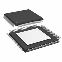
AD9446BSVZ-100 Analog Devices Inc, AD9446BSVZ-100 Datasheet - Page 24

AD9446BSVZ-100
Manufacturer Part Number
AD9446BSVZ-100
Description
IC ADC 16BIT 100MSPS 100-TQFP
Manufacturer
Analog Devices Inc
Datasheet
1.AD9446BSVZ-100.pdf
(36 pages)
Specifications of AD9446BSVZ-100
Data Interface
Parallel
Number Of Bits
16
Sampling Rate (per Second)
100M
Number Of Converters
1
Power Dissipation (max)
2.8W
Voltage Supply Source
Single Supply
Operating Temperature
-40°C ~ 85°C
Mounting Type
Surface Mount
Package / Case
100-TQFP Exposed Pad
Resolution (bits)
16bit
Sampling Rate
100MSPS
Input Channel Type
Differential, Single Ended
Supply Voltage Range - Digital
3V To 3.6V
Supply Current
368mA
Number Of Elements
1
Resolution
16Bit
Architecture
Pipelined
Sample Rate
100MSPS
Input Polarity
Bipolar
Input Type
Voltage
Rated Input Volt
±1/±1.6V
Differential Input
Yes
Power Supply Requirement
Single
Single Supply Voltage (typ)
3.3/5V
Single Supply Voltage (min)
3.14/4.75V
Single Supply Voltage (max)
3.46/5.25V
Dual Supply Voltage (typ)
Not RequiredV
Dual Supply Voltage (min)
Not RequiredV
Dual Supply Voltage (max)
Not RequiredV
Power Dissipation
2.8W
Differential Linearity Error
±0.85LSB
Integral Nonlinearity Error
±6LSB
Operating Temp Range
-40C to 85C
Operating Temperature Classification
Industrial
Mounting
Surface Mount
Pin Count
100
Package Type
TQFP EP
Input Signal Type
Differential
Package
100TQFP EP
Number Of Analog Inputs
1
Digital Interface Type
Parallel
Signal To Noise Ratio
79.7(Typ) dB
Lead Free Status / RoHS Status
Lead free / RoHS Compliant
For Use With
AD9446-80LVDS/PCBZ - BOARD EVALUATION AD9446-80
Lead Free Status / Rohs Status
Compliant
Available stocks
Company
Part Number
Manufacturer
Quantity
Price
Company:
Part Number:
AD9446BSVZ-100
Manufacturer:
AD
Quantity:
138
Company:
Part Number:
AD9446BSVZ-100
Manufacturer:
ADI
Quantity:
132
Part Number:
AD9446BSVZ-100
Manufacturer:
ADI/亚德诺
Quantity:
20 000
AD9446
THEORY OF OPERATION
The AD9446 architecture is optimized for high speed and ease
of use. The analog inputs drive an integrated, high bandwidth
track-and-hold circuit that samples the signal prior to quantization
by the 16-bit pipeline ADC core. The device includes an on-board
reference and input logic that accepts TTL, CMOS, or LVPECL
levels. The digital output logic levels are user selectable as standard
3 V CMOS or LVDS (ANSI-644 compatible) via the OUTPUT
MODE pin.
ANALOG INPUT AND REFERENCE OVERVIEW
A stable and accurate 0.5 V band gap voltage reference is built
into the AD9446. The input range can be adjusted by varying
the reference voltage applied to the AD9446, using either the
internal reference or an externally applied reference voltage.
The input span of the ADC tracks reference voltage changes
linearly.
Internal Reference Connection
A comparator within the AD9446 detects the potential at the
SENSE pin and configures the reference into three possible states,
which are summarized in Table 9. If SENSE is grounded, the
reference amplifier switch is connected to the internal resistor
divider (see Figure 55), setting VREF to ~1.6 V. If a resistor
divider is connected as shown in Figure 56, the switch again sets
to the SENSE pin. This puts the reference amplifier in a
noninverting mode with the VREF output defined as
In all reference configurations, REFT and REFB drive the
analog-to-digital conversion core and establish its input span.
The input range of the ADC always equals twice the voltage at
the reference pin for either an internal or an external reference.
Internal Reference Trim
The internal reference voltage is trimmed during the production
test; therefore, there is little advantage to the user supplying an
external voltage reference to the AD9446. The gain trim is per-
formed with the AD9446 input range set to 3.2 V p-p nominal
(SENSE connected to AGND). Because of this trim and the
maximum ac performance provided by the 3.2 V p-p analog
input range, there is little benefit to using analog input ranges
VREF
=
0
5 .
V
×
⎛ +
⎜
⎝
1
R2
R1
⎞
⎟
⎠
Rev. 0 | Page 24 of 36
<2 V p-p. However, reducing the range can improve SFDR
performance in some applications. Likewise, increasing the
range up to 3.8 V p-p can improve SNR. Users are cautioned
that the differential nonlinearity of the ADC varies with the
reference voltage. Configurations that use <2.0 V p-p may
exhibit missing codes and therefore degraded noise and
distortion performance.
10μF
10μF
+
+
0.1μF
0.1μF
SENSE
Figure 56. Programmable Reference Configuration
VREF
VIN+
VIN–
Figure 55. Internal Reference Configuration
R2
SENSE
R1
VREF
VIN+
VIN–
SELECT
LOGIC
SELECT
AD9446
LOGIC
AD9446
0.5V
CORE
0.5V
ADC
CORE
ADC
REFT
REFB
REFT
REFB
0.1μF
0.1μF
0.1μF
0.1μF
0.1μF
0.1μF
+
10μF
+
10μF


