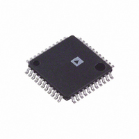
AD9042ASTZ Analog Devices Inc, AD9042ASTZ Datasheet

AD9042ASTZ
Specifications of AD9042ASTZ
Available stocks
Related parts for AD9042ASTZ
AD9042ASTZ Summary of contents
Page 1
FEATURES 41 MSPS minimum sample rate 80 dB spurious-free dynamic range 595 mW power dissipation Single 5 V supply On-chip track-and-hold (T/H) and reference Twos complement output format CMOS-compatible output levels APPLICATIONS Cellular/PCS base stations GPS anti jamming receivers Communications ...
Page 2
AD9042 TABLE OF CONTENTS Features .............................................................................................. 1 Applications ....................................................................................... 1 Functional Block Diagram .............................................................. 1 General Description ......................................................................... 1 Product Highlights ........................................................................... 1 Revision History ............................................................................... 2 Specifications ..................................................................................... 3 DC Specifications ......................................................................... 3 Switching Specifications .............................................................. 4 AC Specifications ...
Page 3
SPECIFICATIONS DC SPECIFICATIONS tied REF OFFSET Table 1. 1 Parameter RESOLUTION DC ACCURACY No Missing Codes Offset Error Offset Tempco Gain Error Gain Tempco 2 REFERENCE OUT (V ) ...
Page 4
AD9042 SWITCHING SPECIFICATIONS = 5 V; ENCODE and ENCODE = 41 MSPS Table 2. 1 Parameter Maximum Conversion Rate Minimum Conversion Rate Aperture Delay ( Aperture Uncertainty (Jitter) ENCODE Pulse Width High ...
Page 5
... All ac specifications tested by driving ENCODE and ENCODE differentially; see the Encoding the AD9042 section for details (Pin 10 on AD9042ASTZ only) tied to GND through a 0.01 μF capacitor. 3 Analog input signal power at −1 dBFS; signal-to-noise ratio (SNR) is the ratio of signal level to total noise (first five harmonics removed). ...
Page 6
AD9042 ABSOLUTE MAXIMUM RATINGS Table 4. 1 Parameter AV Voltage CC DV Voltage CC Analog Input Voltage Analog Input Current Digital Input Voltage (ENCODE) ENCODE, ENCODE Differential Voltage Digital Output Current Operating Temperature Range (Ambient) Maximum Junction Temperature Lead Temperature ...
Page 7
PIN CONFIGURATION AND FUNCTION DESCRIPTIONS Table 6. Pin Function Descriptions Pin No. Mnemonic Description Power Supply (Digital). Powers output stage only ENCODE Encode Input. Data conversion initiated on rising edge. 4 Complement of ...
Page 8
AD9042 TYPICAL PERFORMANCE CHARACTERISTICS 0 –20 –40 – –80 –100 –120 dc 4.1 8.2 12.3 FREQUENCY (MHz) Figure 3. Single Tone at 1.2 MHz 0 –20 –40 – ...
Page 9
ENCODE = 41MSPS –20 AIN = 15.3MHz, 19.5MHz –40 –60 –80 –100 –120 dc 4.1 8.2 12.3 FREQUENCY (MHz) Figure 9. Two Tones at 15.3 MHz and 19.5 MHz 85 AIN = 4.3MHz WORST SPUR SNR ...
Page 10
AD9042 0 ENCODE = 41MSPS AIN = 2.5MHz @ –26dBFS –20 NO DITHER –40 –60 –80 –100 –120 dc 4.1 8.2 12.3 FREQUENCY (MHz) Figure 15. 128K FFT Without Dither 0 ENCODE = 41MSPS AIN = 19.5MHz @ –29dBFS DITHER ...
Page 11
TERMINOLOGY Analog Bandwidth The analog input frequency at which the spectral power of the fundamental frequency (as determined by the FFT analysis) is reduced by 3 dB. Aperture Delay The delay between the 50% point of the rising edge of ...
Page 12
AD9042 EQUIVALENT CIRCUITS t = –250 ps TYP A ANALOG ENCODE INPUTS (ENCODE) DIGITAL OUTPUTS (D11 250µA 250Ω AIN OFFSET 250µA 1.5V Figure 20. Analog Input Stage ...
Page 13
THEORY OF OPERATION The AD9042 analog-to-digital converter (ADC) employs a two- stage subrange architecture. This design approach ensures 12-bit accuracy, without the need for laser trim, at low power. As shown in Figure 1, the 1 V p-p single-ended analog ...
Page 14
AD9042 If no TTL source is available, a clean sine wave can be substituted. In the case of the sine source, the matching network is shown in Figure 29. Because the matching transformer specified is a 1:1 impedance ratio, R, ...
Page 15
When calculating the proper termination resistor, note that the external load resistor is in parallel with the AD9042 analog input resistance, 250 Ω. The external resistor value can be calculated from the following equation ...
Page 16
AD9042 DIGITAL WIDEBAND RECEIVERS INTRODUCTION Several key technologies are now being introduced that may forever alter the vision of radio. Figure 36 shows the typical dual conversion superheterodyne receiver. The signal picked up by the antenna is mixed down to ...
Page 17
Figure 38 shows the block diagram of a typical channelizer. Channelizers consist of a complex NCO (numerically controlled oscillator), dual multiplier (mixer), and matched digital filters. These are the same functions that would be required in an analog receiver but ...
Page 18
AD9042 NOISE FLOOR AND SNR Oversampling is the act of sampling at a rate that is greater than twice the bandwidth of the signal desired. Oversampling has nothing to do with the actual frequency of the sampled signal ...
Page 19
The result can be a marked improvement in the SFDR of the data converter. Figure 16 shows the same converter shown in Figure 13 but with this injection of dither (see Figure 13). SFDR is now 94 dBFS. Figure ...
Page 20
AD9042 Assuming that the C/N ratio must better for accurate demodulation, one of the eight signals can be reduced by 48.8 dB before demodulation becomes unreliable. At this point, the input signal power would be 40.6 ...
Page 21
RECEIVE CHAIN FOR DIGITAL AND ANALOG BEAM FORMING MEDICAL ULTRASOUND USING THE AD9042 The AD9042 is an excellent digitizer for digital and analog beam- forming medical ultrasound systems. The price/performance ratio of the AD9042 allows ultrasound designers the luxury of ...
Page 22
... AD9042 OUTLINE DIMENSIONS 1.45 1.40 1.35 0.15 SEATING 0.05 PLANE VIEW A ROTATED 90° CCW ORDERING GUIDE Model Temperature Range 1 AD9042ASTZ −40°C to +85° RoHS Compliant Part. 12.20 0.75 1.60 12.00 SQ MAX 0.60 11.80 0. PIN 1 TOP VIEW (PINS DOWN) 0.20 0.09 7° ...
Page 23
NOTES Rev Page AD9042 ...
Page 24
AD9042 NOTES ©1995–2009 Analog Devices, Inc. All rights reserved. Trademarks and registered trademarks are the property of their respective owners. D00554-0-9/09(B) Rev Page ...


