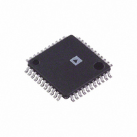
AD9042ASTZ Analog Devices Inc, AD9042ASTZ Datasheet - Page 15

AD9042ASTZ
Manufacturer Part Number
AD9042ASTZ
Description
IC ADC 12BIT 41MSPS 44-TQFP
Manufacturer
Analog Devices Inc
Datasheet
1.AD9042ASTZ.pdf
(24 pages)
Specifications of AD9042ASTZ
Data Interface
Parallel
Number Of Bits
12
Sampling Rate (per Second)
41M
Number Of Converters
3
Power Dissipation (max)
735mW
Voltage Supply Source
Analog and Digital, Dual ±
Operating Temperature
-40°C ~ 85°C
Mounting Type
Surface Mount
Package / Case
44-TQFP, 44-VQFP
Resolution (bits)
12bit
Sampling Rate
41MSPS
Input Channel Type
Single Ended
Supply Voltage Range - Analog
5V
Supply Voltage Range - Digital
5V
Supply Current
119mA
Number Of Elements
1
Resolution
12Bit
Architecture
Pipelined
Sample Rate
41MSPS
Input Polarity
Unipolar
Input Type
Voltage
Rated Input Volt
1.9/2.9V
Differential Input
No
Power Supply Requirement
Single
Single Supply Voltage (typ)
5V
Single Supply Voltage (min)
4.75V
Single Supply Voltage (max)
5.25V
Dual Supply Voltage (typ)
Not RequiredV
Dual Supply Voltage (min)
Not RequiredV
Dual Supply Voltage (max)
Not RequiredV
Power Dissipation
735mW
Differential Linearity Error
±1LSB
Integral Nonlinearity Error
±0.75LSB(Typ)
Operating Temp Range
-40C to 85C
Operating Temperature Classification
Industrial
Mounting
Surface Mount
Pin Count
44
Package Type
LQFP
Input Signal Type
Single-Ended
Lead Free Status / RoHS Status
Lead free / RoHS Compliant
Lead Free Status / RoHS Status
Lead free / RoHS Compliant, Lead free / RoHS Compliant
Available stocks
Company
Part Number
Manufacturer
Quantity
Price
Company:
Part Number:
AD9042ASTZ
Manufacturer:
Analog Devices Inc
Quantity:
10 000
Part Number:
AD9042ASTZ
Manufacturer:
ADI/亚德诺
Quantity:
20 000
When calculating the proper termination resistor, note that the
external load resistor is in parallel with the AD9042 analog
input resistance, 250 Ω. The external resistor value can be
calculated from the following equation:
where Z is desired impedance.
A dc-coupled input configuration (shown in Figure 35) is
limited by the drive amplifier performance. The on-chip
reference of the AD9042 is buffered using the
to-rail operational amplifier. The resulting voltage is combined
with the analog source using an AD9631. Pending improvements
in drive amplifiers, this dc-coupled approach is limited to ~75 dB
to 80 dB of dynamic performance depending on which drive
amplifier is used. The AD9631 and OP279 run off ±5 V.
SOURCE
POWER SUPPLIES
Care should be taken when selecting a power source. Linear
supplies are strongly recommended because switching supplies
tend to have radiated components that may be received by the
AD9042. Each of the power supply pins should be decoupled as
close to the package as possible using 0.1 μF chip capacitors.
The AD9042 has separate digital and analog 5 V pins. The AV
pins are the analog supply pins, and the DV
digital supply pins. Although analog and digital supplies may
be tied together, best performance is achieved when the supplies
are separate. This is because the fast digital output swings can
couple switching noise back into the analog supplies. Note that
AV
SIGNAL
CC
R
must be held within 5% of 5 V.
T
=
21Ω
79Ω
Z
1
−
Figure 35. DC-Coupled Analog Input Circuit
1
250
1
OP279
(1/2)
0.1µF
200Ω
1kΩ
571Ω
AD9631
114Ω
OP279
(1/2)
50Ω
0.1µF
49.9Ω
0pF
TO
50pF
CC
OP279
pins are the
AIN
V
V
AD9042
OFFSET
REF
dual, rail-
Rev. B | Page 15 of 24
CC
OUTPUT LOADING
Care must be taken when designing the data receivers for the
AD9042. It is recommended that the digital outputs drive a
series resistor of 499 Ω followed by a CMOS gate such as the
74AC574. To minimize capacitive loading, there should be only
one gate on each output pin. The digital outputs of the AD9042
have a unique constant slew rate output stage. The output slew
rate is about 1 V/ns independent of output loading. A typical
CMOS gate combined with PCB trace and through hole has a
load of approximately 10 pF. Therefore, as each bit switches, 10 mA
of dynamic current per bit flows in or out of the device. A full-
scale transition can cause up to 120 mA (12 bits × 10 mA/bit) of
current to flow through the digital output stage. The series
resistor minimizes the output currents that can flow in the
output stage. These switching currents are confined between
ground and the DV
avoided because they can appreciably add to the dynamic
switching currents of the AD9042.
LAYOUT INFORMATION
The pinout of the AD9042 facilitates ease of use and the
implementation of high frequency/high resolution design
practices. All of the digital outputs are on one side of the
package, and all of the inputs are on the other sides of the
package. It is highly recommended that high quality ceramic
chip capacitors be used to decouple each supply pin to ground
directly at the device. Depending on the configuration used for
the encode and analog inputs, one or more capacitors are
required on those input pins. The capacitors used on the
ENCODE and V
as noted previously.
Although a multilayer board is recommended, it is not required
to achieve good results. Care should be taken when placing the
digital output runs. Because the digital outputs have such a high
slew rate, the capacitive loading on the digital outputs should be
minimized. Circuit traces for the digital outputs should be kept
short and connected directly to the receiving gate (broken only
by the insertion of the series resistor). Logic fanout for each bit
should be one CMOS gate.
⎛
⎜
⎜
⎝
10
pF
×
1
1
V
ns
REF
⎞
⎟
⎟
⎠
CC
pins must be low inductance chip capacitors
pin. Standard TTL gates should be
AD9042


