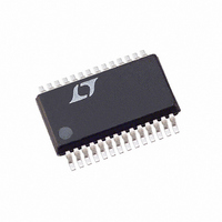
LTC2439-1CGN Linear Technology, LTC2439-1CGN Datasheet - Page 24

LTC2439-1CGN
Manufacturer Part Number
LTC2439-1CGN
Description
IC ADC 16BIT 16CH MCRPWR 28SSOP
Manufacturer
Linear Technology
Datasheet
1.LTC2439-1CGN.pdf
(28 pages)
Specifications of LTC2439-1CGN
Number Of Bits
16
Sampling Rate (per Second)
6.8
Data Interface
MICROWIRE™, Serial, SPI™
Number Of Converters
1
Power Dissipation (max)
1mW
Voltage Supply Source
Single Supply
Operating Temperature
0°C ~ 70°C
Mounting Type
Surface Mount
Package / Case
28-SSOP (0.150", 3.95mm Width)
Lead Free Status / RoHS Status
Contains lead / RoHS non-compliant
Available stocks
Company
Part Number
Manufacturer
Quantity
Price
Part Number:
LTC2439-1CGN
Manufacturer:
LT/凌特
Quantity:
20 000
Part Number:
LTC2439-1CGN#TRPBF
Manufacturer:
LINEAR/凌特
Quantity:
20 000
APPLICATIO S I FOR ATIO
LTC2439-1
IN
gain errors will be insignificant (about 1% of their respec-
tive values over the entire temperature and voltage range).
Even for the most stringent applications, a one-time
calibration operation may be sufficient.
In addition to the input sampling charge, the input ESD
protection diodes have a temperature dependent leakage
current. This current, nominally 1nA (±10nA max), results
in a small offset shift. A 15k source resistance will create
a 0LSB typical and 1LSB maximum offset voltage.
Reference Current
In a similar fashion, the LTC2439-1 samples the differen-
tial reference pins REF
of charge to and from the external driving circuits thus
producing a dynamic reference current. This current does
not change the converter offset, but it may degrade the
gain and INL performance. The effect of this current can be
analyzed in the same two distinct situations.
For relatively small values of the external reference capaci-
tors (C
settles almost completely and relatively large values for
the source impedance result in only small errors. Such
values for C
gain performance without significant benefits of reference
filtering and the user is advised to avoid them.
Larger values of reference capacitors (C
be required as reference filters in certain configurations.
Such capacitors will average the reference sampling charge
24
Figure 19. +FS Error vs R
–
, the expected drift of the dynamic current, offset and
REF
< 0.01µF), the voltage on the sampling capacitor
REF
–1
–2
–3
0
1
V
REF
REF
IN
IN
F
T
will deteriorate the converter offset and
O
A
CC
+
–
= GND
= 25°C
+
–
= 5V
= 5V
= 2.5V
U
= 5V
= GND
C
10
REF
+
C
REF
C
and REF
C
REF
= 0.001µF
REF
SOURCE
= 100pF
= 0.01µF
U
R
= 0pF
100
SOURCE
–
at REF
transferring small amount
(Ω)
1k
W
+
or REF
10k
REF
24361 F19
> 0.01µF) may
–
100k
(Small C
U
IN
)
and the external source resistance will see a quasi con-
stant reference differential impedance. When F
(internal oscillator and 50Hz/60Hz notch), the typical
differential reference resistance is 1.4MΩ which will gen-
erate a gain error of approximately 1LSB full scale for each
40Ω of source resistance driving REF
is driven by an external oscillator with a frequency f
(external conversion clock operation), the typical differen-
tial reference resistance is 0.20 • 10
ohm of source resistance driving REF
in 1.54 • 10
of the source resistance on the two reference pins is
additive with respect to this gain error. The typical +FS and
–FS errors for various combinations of source resistance
seen by the REF
C
21 and 22.
In addition to this gain error, the converter INL perfor-
mance is degraded by the reference source impedance.
When F
every 1000Ω of source resistance driving REF
translates into about 1LSB additional INL error. When F
is driven by an external oscillator with a frequency f
every 100Ω of source resistance driving REF
translates into about 5.5 • 10
error. Figure 23 shows the typical INL error due to the
source resistance driving the REF
large C
resistance on the two reference pins is additive with
respect to this INL error. In general, matching of source
REF
Figure 20. –FS Error vs R
connected to these pins are shown in Figures 19, 20,
O
REF
= LOW (internal oscillator and 50Hz/60Hz notch),
–7
values are used. The effect of the source
3
2
1
0
• f
1
EOSC
+
V
REF
REF
IN
IN
F
T
O
A
CC
+
and REF
–
= GND
= 25°C
+
= GND
= 5V
–
= 2.5V
C
= 5V
= GND
LSB gain error at full scale. The effect
10
REF
C
C
REF
REF
= 0.001µF
C
REF
SOURCE
= 100pF
= 0.01µF
–
100
R
= 0pF
SOURCE
pins and external capacitance
–7
at REF
• f
(Ω)
1k
EOSC
+
+
12
or REF
+
+
or REF
10k
LSB additional INL
/f
or REF
or REF
EOSC
2412 F19
100k
–
–
Ω and each
(Small C
–
–
pins when
. When F
+
+
will result
O
or REF
or REF
= LOW
EOSC
24391fa
EOSC
IN
)
O
O
–
–
,


