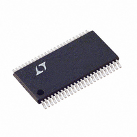
LTC1851CFW Linear Technology, LTC1851CFW Datasheet - Page 10

LTC1851CFW
Manufacturer Part Number
LTC1851CFW
Description
IC ADC 12BIT 1.25MSPS 48-TSSOP
Manufacturer
Linear Technology
Datasheet
1.LTC1851CFWPBF.pdf
(28 pages)
Specifications of LTC1851CFW
Number Of Bits
12
Sampling Rate (per Second)
1.25M
Data Interface
Parallel
Number Of Converters
1
Power Dissipation (max)
50mW
Voltage Supply Source
Single Supply
Operating Temperature
0°C ~ 70°C
Mounting Type
Surface Mount
Package / Case
48-TFSOP (0.240", 6.10mm Width)
Lead Free Status / RoHS Status
Contains lead / RoHS non-compliant
Available stocks
Company
Part Number
Manufacturer
Quantity
Price
Company:
Part Number:
LTC1851CFW
Manufacturer:
ABOV
Quantity:
270
Part Number:
LTC1851CFW
Manufacturer:
LT/凌特
Quantity:
20 000
Company:
Part Number:
LTC1851CFW#PBF
Manufacturer:
AD
Quantity:
21
CH0 to CH7 (Pins 1 to 8): Analog Input Pins. Input pins can
be used single ended relative to the analog input common
pin (COM) or differentially in pairs (CH0 and CH1, CH2 and
CH3, CH4 and CH5, CH6 and CH7).
COM (Pin 9): Analog Input Common Pin. For single-ended
operation (DIFF = 0), COM is the “–” analog input. COM is
disabled when DIFF is high.
REFOUT (Pin 10): Internal 2.5V Reference Output. Re-
quires bypass to analog ground plane with 1 F.
REFIN (Pin 11): Reference Mode Select/Reference Buffer
Input. REFIN selects the Reference mode and acts as the
reference buffer Input. REFIN tied to ground will produce
2.048V on the REFCOMP pin. REFIN tied to the positive
supply disables the reference buffer to allow REFCOMP to
be driven externally. For voltages between 1V and 2.6V,
the reference buffer produces an output voltage on the
REFCOMP pin equal to 1.6384 times the voltage on REFIN
(4.096V on REFCOMP for a 2.5V input on REFIN).
REFCOMP (Pin 12): Reference Buffer Output. REFCOMP
sets the full-scale input span. The reference buffer pro-
duces an output voltage on the REFCOMP pin equal to
1.6384 times the voltage on the REFIN pin (4.096V on
REFCOMP for a 2.5V input on REFIN). REFIN tied to
ground will produce 2.048V on the REFCOMP pin.
REFCOMP can be driven externally if REFIN is tied to the
positive supply. Requires bypass to analog ground plane
with 10 F tantalum in parallel with 0.1 F ceramic or 10 F
ceramic.
GND (Pin 13): Ground. Tie to analog ground plane.
V
V
tantalum in parallel with 0.1 F ceramic or 10 F ceramic.
GND (Pin 16): Ground for Internal Logic. Tie to analog
ground plane.
DIFF
Active when RD is low. Following a conversion, the single-
ended/differential bit of the present conversion is available
on this pin concurrent with the conversion result. In
Readback mode, the single-ended/differential bit of the
LTC1850/LTC1851
PI FU CTIO S
10
DD
DD
U
(Pin 14): 5V Supply. Short to Pin 15.
OUT
(Pin 15): 5V Supply. Bypass to GND with 10 F
/S6 (Pin 17): Three-State Digital Data Output.
U
U
current sequencer location (S6) is available on this pin.
The output swings between OV
A2
State Digital MUX Address Outputs. Active when RD is
low. Following a conversion, the MUX address of the
present conversion is available on these pins concurrent
with the conversion result. In Readback mode, the MUX
address of the current sequencer location (S5-S3) is
available on these pins. The outputs swing between OV
and OGND.
D9/S2 (Pin 21, LTC1850): Three-State Digital Data Out-
put. Active when RD is low. Following a conversion, bit 9
of the present conversion is available on this pin. In
Readback mode, the unipolar/bipolar bit of the current
sequencer location (S2) is available on this pin. The output
swings between OV
D11/S2 (Pin 21, LTC1851): Three-State Digital Data Out-
put. Active when RD is low. Following a conversion, bit 11
of the present conversion is available on this pin. In
Readback mode, the unipolar/bipolar bit of the current
sequencer location (S2) is available on this pin. The output
swings between OV
D8/S1 (Pin 22, LTC1850): Three-State Digital Data Out-
puts. Active when RD is low. Following a conversion, bit 8
of the present conversion is available on this pin. In
Readback mode, the gain bit of the current sequencer
location (S1) is available on this pin. The output swings
between OV
D10/S1 (Pin 22, LTC1851): Three-State Digital Data Out-
puts. Active when RD is low. Following a conversion, bit 10
of the present conversion is available on this pin. In
Readback mode, the gain bit of the current sequencer
location (S1) is available on this pin. The output swings
between OV
D7/S0 (Pin 23, LTC1850): Three-State Digital Data Out-
puts. Active when RD is low. Following a conversion, bit 7
of the present conversion is available on this pin. In
Readback mode, the end of sequence bit of the current
sequencer location (S0) is available on this pin. The output
swings between OV
OUT
/S5, A1
DD
DD
OUT
and OGND.
and OGND.
/S4, A0
DD
DD
DD
and OGND.
and OGND.
and OGND.
OUT
/S3 (Pins 18 to 20): Three-
DD
and OGND.
18501f
DD


