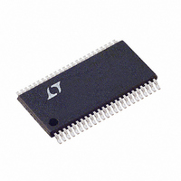
LTC1851CFW Linear Technology, LTC1851CFW Datasheet - Page 24

LTC1851CFW
Manufacturer Part Number
LTC1851CFW
Description
IC ADC 12BIT 1.25MSPS 48-TSSOP
Manufacturer
Linear Technology
Datasheet
1.LTC1851CFWPBF.pdf
(28 pages)
Specifications of LTC1851CFW
Number Of Bits
12
Sampling Rate (per Second)
1.25M
Data Interface
Parallel
Number Of Converters
1
Power Dissipation (max)
50mW
Voltage Supply Source
Single Supply
Operating Temperature
0°C ~ 70°C
Mounting Type
Surface Mount
Package / Case
48-TFSOP (0.240", 6.10mm Width)
Lead Free Status / RoHS Status
Contains lead / RoHS non-compliant
Available stocks
Company
Part Number
Manufacturer
Quantity
Price
Company:
Part Number:
LTC1851CFW
Manufacturer:
ABOV
Quantity:
270
Part Number:
LTC1851CFW
Manufacturer:
LT/凌特
Quantity:
20 000
Company:
Part Number:
LTC1851CFW#PBF
Manufacturer:
AD
Quantity:
21
APPLICATIO S I FOR ATIO
Table 5
OPERATION MODE
Direct Address
Scan
Program
Readback
Sequence Run
LTC1850/LTC1851
Sequence Run Mode
Once the sequencer is programmed, M0 is taken high.
BUSY will also come back high enabling CONVST and the
next falling CONVST will begin a conversion using the
MUX address and input configuration stored in location
0000 of the sequencer memory. After each conversion, the
sequencer pointer is advanced by one and the MUX
address (the actual channel or channels being converted,
not the sequencer pointer) for the present conversion is
available on the address output pins along with the con-
version result. When the sequencer finishes converting
the last programmed location, the sequencer pointer will
return to location 0000 for the next conversion. The
24
U
M1
0
0
0
0
1
1
1
U
M0
0
0
1
1
0
0
1
WR
0
0
1
X
W
RD
OE
OE
OE
OE
OE
1
U
COMMENTS
Address and Configuration are Driven from External Pins
Address and Configuration are Latched on Rising Edge of WR or Falling Edge of CONVST
Address is Provided by Internal Scan Counter, Configuration is Driven from External Pins
Configuration is Latched on Rising Edge of WR or Falling Edge of CONVST
Write Sequencer Location, WR Low Enables Inputs, Rising Edge of WR Latches Data and
Advances to Next Location
Read Sequencer Location, Falling Edge of RD Enables Output, Rising Edge of RD
Advances to Next Location
Run Programmed Sequence, Falling Edge of CONVST Starts Conversion and Advances to
Next Location
sequencer will also reset to location 0000 anytime the M1
or M0 pin changes state.
The contents of the sequencer memory will be retained as
long as power is continuously applied to the part. This
allows the user to switch from Sequence Run mode to
either Direct Address or Scan Mode and back without
losing the programmed sequence. The part can also be
disabled using CS or shutdown in Nap or Sleep mode
without losing the programmed sequence. Table 5 out-
lines the operational modes of the LTC1850/LTC1851.
Figures 11 and 12 show the timing diagrams for writing to,
reading from and running a sequence with the LTC1850/
LTC1851.
18501f


