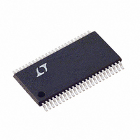
LTC1851CFW Linear Technology, LTC1851CFW Datasheet - Page 23

LTC1851CFW
Manufacturer Part Number
LTC1851CFW
Description
IC ADC 12BIT 1.25MSPS 48-TSSOP
Manufacturer
Linear Technology
Datasheet
1.LTC1851CFWPBF.pdf
(28 pages)
Specifications of LTC1851CFW
Number Of Bits
12
Sampling Rate (per Second)
1.25M
Data Interface
Parallel
Number Of Converters
1
Power Dissipation (max)
50mW
Voltage Supply Source
Single Supply
Operating Temperature
0°C ~ 70°C
Mounting Type
Surface Mount
Package / Case
48-TFSOP (0.240", 6.10mm Width)
Lead Free Status / RoHS Status
Contains lead / RoHS non-compliant
Available stocks
Company
Part Number
Manufacturer
Quantity
Price
Company:
Part Number:
LTC1851CFW
Manufacturer:
ABOV
Quantity:
270
Part Number:
LTC1851CFW
Manufacturer:
LT/凌特
Quantity:
20 000
Company:
Part Number:
LTC1851CFW#PBF
Manufacturer:
AD
Quantity:
21
APPLICATIO S I FOR ATIO
The sequencer is accessed by taking the M1 mode pin
high. With M1 high, the sequencer memory is accessed by
taking the M0 mode pin low. This will cause BUSY to go
low, disabling conversions during the programming and
readback of the sequencer. The sequencer is reset to
location 0000 whenever M1 or M0 changes state. One of
these signals should be cycled prior to any read or write
operation to guarantee that the sequencer will be pro-
grammed or read starting at location 0000.
The sequencer is programmed sequentially starting from
location 0000. RD and WR should be held high, the
appropriate signals applied to the DIFF pin, the A2 to A0
MUX address pins, the UNI/BIP pin and the PGA pin and
WR taken low to write to the memory. The rising edge of
WR will latch the data into memory and advance the
pointer to the next sequencer location. Up to 16 locations
can be programmed and the last location written before
M0 is taken back high will be the last location in the
sequence. After 16 writes, the pointer is reset to location
0000 and any subsequent writes will overwrite the previ-
ous contents and start a new sequence.
U
LOCATION 0000
LOCATION 0001
LOCATION 0010
LOCATION 1110
LOCATION 1111
U
W
DIFF
S6
•
•
•
Figure 10. Sequencer Memory Block Diagram
S5
A2
•
•
•
U
S4
A1
•
•
•
S3
A0
•
•
•
The sequencer memory can be read by holding WR high
and driving RD. Taking RD low accesses the sequencer
memory and enables the data output pins. The sequencer
should be reset to location 0000 (by pulsing M0 high)
before beginning a read operation. The seven output bits
will be available on the DIFF
A0
DIFF
S1 and D7/S0 pins (LTC1850). The D8 to D0 (LTC1851) or
D6 to D0 (LTC1850) data output pins will remain high
impedance during readback. RD going high will return the
data output pins to a high impedance state and advance the
pointer to the next location. A logic 1 on the D9/S0 (or D7/
S0) pin indicates the last location in the current sequence
but all 16 locations can be read by continuing to clock RD.
After 16 reads, the pointer is reset to location 0000. When
all programming and/or reading of the sequencer memory
is complete, M0 is taken high. BUSY will come back high
enabling CONVST and indicating that the part is ready to
start a conversion.
UNI/BIP
OUT
S2
•
•
•
OUT
/S3, D11/S2, D10/S1 and D9/S0 pins (LTC1851) or
/S6, A2
PGA
S1
•
•
•
EOS
OUT
S0
1851 F10
•
•
•
/S5, A1
LTC1850/LTC1851
OUT
OUT
/S4, A0
/S6, A2
OUT
OUT
/S3, D9/S2, D8/
/S5, A1
OUT
23
/S4,
18501f


