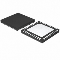
LTC2259CUJ-14#TRPBF Linear Technology, LTC2259CUJ-14#TRPBF Datasheet - Page 15

LTC2259CUJ-14#TRPBF
Manufacturer Part Number
LTC2259CUJ-14#TRPBF
Description
IC ADC 14BIT 80MSPS 40-QFN
Manufacturer
Linear Technology
Datasheet
1.LTC2259IUJ-14PBF.pdf
(32 pages)
Specifications of LTC2259CUJ-14#TRPBF
Number Of Bits
14
Sampling Rate (per Second)
80M
Data Interface
Serial, Parallel
Number Of Converters
1
Power Dissipation (max)
105mW
Voltage Supply Source
Single Supply
Operating Temperature
0°C ~ 70°C
Mounting Type
Surface Mount
Package / Case
40-WFQFN Exposed Pad
Lead Free Status / RoHS Status
Lead free / RoHS Compliant
Available stocks
Company
Part Number
Manufacturer
Quantity
Price
PIN FUNCTIONS
operating modes. PAR/SER should be connected directly
to ground or the V
logic signal.
V
to ground with 0.1μF ceramic capacitors. Pins 9 and 10
can share a bypass capacitor.
ENC
rising edge.
ENC
starts on the falling edge.
CS (Pin 13): In serial programming mode, (PAR/SER =
0V), CS is the serial interface chip select input. When
CS is low, SCK is enabled for shifting data on SDI into
the mode control registers. In the parallel programming
mode (PAR/SER = V
stabilizer. When CS is low, the clock duty cycle stabilizer is
turned off. When CS is high, the clock duty cycle stabilizer
is turned on. CS can be driven with 1.8V to 3.3V logic.
SCK (Pin 14): In serial programming mode, (PAR/SER =
0V), SCK is the serial interface clock input. In the parallel
programming mode (PAR/SER = V
digital output mode. When SCK is low, the full-rate CMOS
output mode is enabled. When SCK is high, the double-
data rate LVDS output mode (with 3.5mA output current)
is enabled. SCK can be driven with 1.8V to 3.3V logic.
SDI (Pin 15): In serial programming mode, (PAR/SER =
0V), SDI is the serial interface data input. Data on SDI is
clocked into the mode control registers on the rising edge
of SCK. In the parallel programming mode (PAR/SER =
V
is low, the part operates normally. When SDI is high, the
part enters sleep mode. SDI can be driven with 1.8V to
3.3V logic.
SDO (Pin 16): In serial programming mode, (PAR/SER
= 0V), SDO is the optional serial interface data output.
Data on SDO is read back from the mode control registers
and can be latched on the falling edge of SCK. SDO is an
open-drain NMOS output that requires an external 2k
pull-up resistor to 1.8V-3.3V. If read back from the mode
control registers is not needed, the pull-up resistor is not
necessary and SDO can be left unconnected. In the parallel
programming mode (PAR/SER = V
and should not be connected.
DD
DD
), SDI can be used to power down the part. When SDI
+
–
(Pins 9, 10, 40): 1.8V Analog Power Supply. Bypass
(Pin 11): Encode Input. Conversion starts on the
(Pin 12): Encode Complement Input. Conversion
DD
DD
of the part and not be driven by a
), CS controls the clock duty cycle
DD
DD
), SCK controls the
), SDO is not used
OGND (Pin 25): Output Driver Ground.
OV
with a 0.1μF ceramic capacitor.
V
Equal to V
mode of the analog inputs. Bypass to ground with a 0.1μF
ceramic capacitor.
V
with a 1μF ceramic capacitor, nominally 1.25V.
SENSE (Pin 39): Reference Programming Pin. Connecting
SENSE to V
range. Connecting SENSE to ground selects the internal
reference and a ±0.5V input range. An external reference
between 0.625V and 1.3V applied to SENSE selects an
input range of ±0.8 • V
FULL-RATE CMOS OUTPUT MODE
All Pins Below Have CMOS Output Levels (OGND to
OV
D0 to D13 (Pins 17-24, 29-34): Digital Outputs. D13 is
the MSB.
CLKOUT
CLKOUT
normally transition at the same time as the falling edge
of CLKOUT
relative to the digital outputs by programming the mode
control registers.
DNC (Pin 35): Do not connect this pin.
OF (Pin 36): Over/Under Flow Digital Output. OF is high
when an overfl ow or underfl ow has occurred.
DOUBLE-DATA RATE CMOS OUTPUT MODE
All Pins Below Have CMOS Output Levels (OGND to
OV
D0_1 to D12_13 (Pins 18, 20, 22, 24, 30, 32, 34): Double-
Data Rate Digital Outputs. Two data bits are multiplexed onto
each output pin. The even data bits (D0, D2, D4, D6, D8, D10,
CM
REF
DD
DD
DD
(Pin 38): Reference Voltage Output. Bypass to ground
(Pin 37): Common Mode Bias Output, Nominally
)
)
(Pin 26): Output Driver Supply. Bypass to ground
LTC2260-14/LTC2259-14
–
+
(Pin 28): Data Output Clock. The digital outputs
DD
(Pin 27): Inverted Version of CLKOUT
DD
+
. The phase of CLKOUT
/2. V
selects the internal reference and a ±1V input
CM
should be used to bias the common
SENSE
.
LTC2261-14
+
can also be delayed
+
15
.
226114fa


