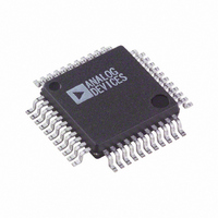
AD7859ASZ Analog Devices Inc, AD7859ASZ Datasheet - Page 12

AD7859ASZ
Manufacturer Part Number
AD7859ASZ
Description
IC ADC 12BIT 8CH LP 44-MQFP
Manufacturer
Analog Devices Inc
Datasheet
1.AD7859LASZ.pdf
(28 pages)
Specifications of AD7859ASZ
Data Interface
Parallel
Number Of Bits
12
Sampling Rate (per Second)
200k
Number Of Converters
2
Power Dissipation (max)
30mW
Voltage Supply Source
Analog and Digital
Operating Temperature
-40°C ~ 85°C
Mounting Type
Surface Mount
Package / Case
44-MQFP, 44-PQFP
Resolution (bits)
12bit
Sampling Rate
100kSPS
Input Channel Type
Single Ended
Supply Voltage Range - Analog
3V To 5.5V
Supply Voltage Range - Digital
3V To 5.5V
Lead Free Status / RoHS Status
Lead free / RoHS Compliant
Available stocks
Company
Part Number
Manufacturer
Quantity
Price
Company:
Part Number:
AD7859ASZ
Manufacturer:
Analog Devices Inc
Quantity:
10 000
Part Number:
AD7859ASZ
Manufacturer:
ADI/亚德诺
Quantity:
20 000
Company:
Part Number:
AD7859ASZ-REEL
Manufacturer:
Analog Devices Inc
Quantity:
10 000
AD7859/AD7859L
CALIBRATION REGISTERS
The AD7859/AD7859L has 10 calibration registers in all, 8 for the DAC, 1 for offset and 1 for gain. Data can be written to or read
from all 10 calibration registers. In self and system calibration, the part automatically modifies the calibration registers; only if the
user needs to modify the calibration registers should an attempt be made to read from and write to the calibration registers.
Addressing the Calibration Registers
The calibration selection bits in the control register CALSLT1 and CALSLT0 determine which of the calibration registers are ad-
dressed (See Table V). The addressing applies to both the read and write operations for the calibration registers. The user should not
attempt to read from and write to the calibration registers at the same time.
CALSLT1
0
0
1
1
Writing to/Reading from the Calibration Registers
When writing to the calibration registers a write to the control
register is required to set the CALSLT0 and CALSLT1 bits.
When reading from the calibration registers a write to the con-
trol register is required to set the CALSLT0 and CALSLT1 bits
and also to set the RDSLT1 and RDSLT0 bits to 10 (this ad-
dresses the calibration registers for reading). The calibration
register pointer is reset on writing to the control register setting
the CALSLT1 and CALSLT0 bits, or upon completion of all
the calibration register write/read operations. When reset it
points to the first calibration register in the selected write/read
sequence. The calibration register pointer points to the gain
calibration register upon reset in all but one case, this case being
where the offset calibration register is selected on its own
(CALSLT1 = 1, CALSLT0 = 0). Where more than one cali-
bration register is being accessed, the calibration register pointer
is automatically incremented after each full calibration register
write/read operation. The calibration register address pointer is
incremented after the high byte read or write operation in byte
mode. Therefore when reading (in byte mode) from the calibra-
tion registers, the low byte must always be read first, i.e., HBEN
= logic zero. The order in which the 10 calibration registers are
arranged is shown in Figure 5. Read/Write operations may be
aborted at any time before all the calibration registers have been
accessed, and the next control register write operation resets the
calibration register pointer. The flowchart in Figure 6 shows the
sequence for writing to the calibration registers. Figure 7 shows
the sequence for reading from the calibration registers.
ADDRESS POINTER
Figure 5. Calibration Register Arrangement
CALIBRATION REGISTER ADDRESS POINTER POSITION IS
DETERMINED BY THE NUMBER OF CALIBRATION REGISTERS
ADDRESSED AND THE NUMBER OF READ/WRITE OPERATIONS.
CAL REGISTER
CALSLT0
0
1
0
1
Comment
This combination addresses the Gain (1), Offset (1) and DAC Registers (8). Ten registers in total.
This combination addresses the Gain (1) and Offset (1) Registers. Two registers in total.
This combination addresses the Offset Register. One register in total.
This combination addresses the Gain Register. One register in total.
CALIBRATION REGISTERS
DAC 1st MSB REGISTER
DAC 8th MSB REGISTER
OFFSET REGISTER
GAIN REGISTER
Table V. Calibration Register Addressing
(1)
(2)
(3)
(10)
–12–
When reading from the calibration registers there is always two
leading zeros for each of the registers.
Figure 6. Flowchart for Writing to the Calibration Registers
WRITE TO CONTROL REGISTER SETTING STCAL = 0
AND CALSLT1, CALSLT0 = 00, 01, 10, 11
AUTOMATICALLY INCREMENTED
CAL REGISTER POINTER IS
CAL REGISTER POINTER IS
WRITE TO CAL REGISTER
AUTOMATICALLY RESET
(ADDR1 = 1, ADDR0 = 0)
OPERATION
REGISTER
FINISHED
ABORT
START
WRITE
LAST
OR
?
YES
NO
REV. A


