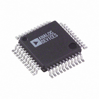
AD7859ASZ Analog Devices Inc, AD7859ASZ Datasheet - Page 19

AD7859ASZ
Manufacturer Part Number
AD7859ASZ
Description
IC ADC 12BIT 8CH LP 44-MQFP
Manufacturer
Analog Devices Inc
Datasheet
1.AD7859LASZ.pdf
(28 pages)
Specifications of AD7859ASZ
Data Interface
Parallel
Number Of Bits
12
Sampling Rate (per Second)
200k
Number Of Converters
2
Power Dissipation (max)
30mW
Voltage Supply Source
Analog and Digital
Operating Temperature
-40°C ~ 85°C
Mounting Type
Surface Mount
Package / Case
44-MQFP, 44-PQFP
Resolution (bits)
12bit
Sampling Rate
100kSPS
Input Channel Type
Single Ended
Supply Voltage Range - Analog
3V To 5.5V
Supply Voltage Range - Digital
3V To 5.5V
Lead Free Status / RoHS Status
Lead free / RoHS Compliant
Available stocks
Company
Part Number
Manufacturer
Quantity
Price
Company:
Part Number:
AD7859ASZ
Manufacturer:
Analog Devices Inc
Quantity:
10 000
Part Number:
AD7859ASZ
Manufacturer:
ADI/亚德诺
Quantity:
20 000
Company:
Part Number:
AD7859ASZ-REEL
Manufacturer:
Analog Devices Inc
Quantity:
10 000
REV. A
Figure 21. Using the CONVST Pin to Power Up the AD7859
for a Conversion
Using The Internal (On-Chip) Reference
As in the case of an external reference, the AD7859/AD7859L
can power up from one of two conditions, power-up after the
supplies are connected or power-up from hardware/software
power-down.
When using the on-chip reference and powering up when AV
and DV
power-up calibration mode be disabled as explained above.
When using the on-chip reference, the power-up time is effec-
tively the time it takes to charge up the external capacitor on the
REF
where R
The recommended value of the external capacitor is 100 nF;
this gives a power-up time of approximately 135 ms before a
calibration is initiated and normal operation should commence.
When C
or software power-down reduces to 5 s. This is because an in-
ternal switch opens to provide a high impedance discharge path
for the reference capacitor during power-down—see Figure 22.
An added advantage of the low charge leakage from the refer-
ence capacitor during power-down is that even though the refer-
ence is being powered down between conversions, the reference
capacitor holds the reference voltage to within 0.5 LSBs with
throughput rates of 100 samples/second and over with a full
power-down between conversions. A high input impedance op
amp like the AD707 should be used to buffer this reference
capacitor if it is being used externally. Note, if the AD7859/
AD7859L is left in its powered-down state for more than
100 ms, the charge on C
power-up time will increase. If this long power-up time is a
problem, the user can use a partial power-down for the last con-
version so the reference remains powered up.
CONVST
BUSY
Figure 22. On-Chip Reference During Power-Down
IN
CAPACITOR
/REF
EXTERNAL
DD
REF
150K and C = external capacitor.
are first connected, it is recommended that the
OUT
is fully charged, the power-up time from a hardware
REF
pin. This time is given by the equation:
IN/OUT
POWER-UP
TIME
5µs
DURING POWER-DOWN
POWER UP ON FALLING EDGE
REF
t
UP
SWITCH OPENS
OPERATION
= 9
will start to leak away and the
t
NORMAL
START CONVERSION ON RISING EDGE
CONVERT
4.6µs
R
C
POWER-DOWN
REFERENCE
ON-CHIP
BUF
FULL
CIRCUITRY
TO OTHER
POWER-UP
TIME
DD
–19–
POWER VS. THROUGHPUT RATE
The main advantage of a full power-down after a conversion is
that it significantly reduces the power consumption of the part
at lower throughput rates. When using this mode of operation,
the AD7859/AD7859L is only powered up for the duration of
the conversion. If the power-up time of the AD7859/AD7859L
is taken to be 5 s and it is assumed that the current during
power up is 4.5 mA/1.5 mA typ, then power consumption as a
function of throughput can easily be calculated. The AD7859
has a conversion time of 4.6 s with a 4 MHz external clock and
the AD7859L has a conversion time of 9 s with a 1.8 MHz
clock. This means the AD7859/AD7859L consumes 4.5 mA/
1.5 mA typ for 9.6 s/14 s in every conversion cycle if the parts
are powered down at the end of a conversion. The two graphs,
Figure 24 and Figure 25, show the power consumption of the
AD7859 and AD7859L for V
put. Table VIII lists the power consumption for various
throughput rates.
Throughput Rate
1 kSPS
10 kSPS
20 kSPS
50 kSPS
0V TO 2.5V
ANALOG
SUPPLY
INPUT
+3V
Table VIII. Power Consumption vs. Throughput
REFERENCE
DV
EXTERNAL
OPTIONAL
I = 1.5mA TYP
DD
0.01µF
Figure 23. Typical Low Power Circuit
CURRENT,
0.1µF
10µF
REF192
AIN(+)
AIN(–)
C
C
SLEEP
CAL
AGND
DGND
REF1
REF2
0.1µF
AV
REF
AD7859L
DD
DD
Power
AD7859
130 W
1.3 mW
2.6 mW
6.48 mW
IN
/REF
DV
AD7859/AD7859L
= 3 V as a function of through-
DD
0.1µF
OUT
0.1µF
CONVST
CLKIN
BUSY
DB15
W/B
DB0
WR
RD
CS
OSCILLATOR
1.8MHz
START SIGNAL
CONVERSION
Power
AD7859L
65 W
650 W
1.25 mW
3.2 mW
POWER
µC/µP
LOW


