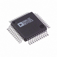
AD7859ASZ Analog Devices Inc, AD7859ASZ Datasheet - Page 24

AD7859ASZ
Manufacturer Part Number
AD7859ASZ
Description
IC ADC 12BIT 8CH LP 44-MQFP
Manufacturer
Analog Devices Inc
Datasheet
1.AD7859LASZ.pdf
(28 pages)
Specifications of AD7859ASZ
Data Interface
Parallel
Number Of Bits
12
Sampling Rate (per Second)
200k
Number Of Converters
2
Power Dissipation (max)
30mW
Voltage Supply Source
Analog and Digital
Operating Temperature
-40°C ~ 85°C
Mounting Type
Surface Mount
Package / Case
44-MQFP, 44-PQFP
Resolution (bits)
12bit
Sampling Rate
100kSPS
Input Channel Type
Single Ended
Supply Voltage Range - Analog
3V To 5.5V
Supply Voltage Range - Digital
3V To 5.5V
Lead Free Status / RoHS Status
Lead free / RoHS Compliant
Available stocks
Company
Part Number
Manufacturer
Quantity
Price
Company:
Part Number:
AD7859ASZ
Manufacturer:
Analog Devices Inc
Quantity:
10 000
Part Number:
AD7859ASZ
Manufacturer:
ADI/亚德诺
Quantity:
20 000
Company:
Part Number:
AD7859ASZ-REEL
Manufacturer:
Analog Devices Inc
Quantity:
10 000
AD7859/AD7859L
PARALLEL INTERFACE
The AD7859 provides a flexible, high speed, parallel interface.
This interface is capable of operating in either word (with the
W/B pin tied high) or byte (with W/B tied low) mode. A detailed
description of the different interface arrangements follows.
Reading
With the W/B pin at a logic high, the AD7859 interface operates
in word mode. In this case, a single read operation from the
device accesses the word on pins DB0 to DB15 (for a data read,
the 12-bit conversion result appears on DB0–DB11). DB0 is
the LSB of the word. The DB8/HBEN pin assumes its DB8
function. With the W/B pin at a logic low, the AD7859 interface
operates in byte mode. In this case, the DB8/HBEN pin as-
sumes its HBEN function. Data to be accessed from the
AD7859 must be accessed in two read operations with 8 bits of
data provided by the AD7859 on DB0–DB7 for each of the
read operations. The HBEN pin determines whether the read
operation accesses the high byte or low byte of the 16-bit word.
For a low byte read, DB0 provides the LSB of the 16-bit word.
For a high byte read DB0 provides data bit 8 of the 16-bit word
with DB7 providing the MSB of the 16-bit word.
DB0 – DB15
DB0 – DB7
INTERNAL
CONVST
LATCH
Figure 35. Read and Write Cycle Timing Diagram for 16-Bit Transfers
HBEN
BUSY
DATA
RD
WR
CS
CS
RD
*
W/B PIN LOGIC LOW
*
Figure 36. Read Cycle Timing for Byte Mode Operation
W/B PIN LOGIC HIGH
t
13
t
3
t
5
OLD DATA
t
VALID
DATA
t
15
t
8
16
LOW BYTE
t
7
t
17
t
14
t
t
9
6
–24–
t
4
Figure 35 shows the read cycle timing diagram for 16-bit trans-
fers for the AD7859. When operated in word mode, the HBEN
input does not exist, and only the first read operation is required
to access data from the AD7859. Valid data, in this case, is pro-
vided on DB0–DB15. When operated in byte mode, the two
read cycles shown in Figure 36 are required to access the full data
word from the AD7859. Note that in byte mode, the order of
successive read operations is important when reading the cali-
bration registers. This is because the register file address pointer
is incremented on a high byte read as explained in the calibra-
tion register section of this data sheet. In this case the order of
the read should always be Low Byte–High Byte. In Figure 36,
the first read places the lower 8 bits of the full data word on
DB0–DB7 and the second read places the upper 8 bits of the
data word on DB0–DB7.
The CS and RD signals are gated internally and level-triggered
active low. In either word or byte mode, CS and RD may be
tied together as the timing specification for t
The data is output a time t
RD rising should be used to latch data by the user and after a
time t
t
1
t
t
10
CONVERT
9
the data lines will become three-stated.
t
3
t
t
18
5
t
8
HIGH BYTE
NEW DATA
t
VALID
DATA
7
8
after both CS and RD go low. The
t
4
t
9
t
6
5
and t
6
is 0 ns min.
REV. A


