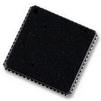
AD9255BCPZ-80 Analog Devices Inc, AD9255BCPZ-80 Datasheet - Page 3

AD9255BCPZ-80
Manufacturer Part Number
AD9255BCPZ-80
Description
IC ADC 14BIT 80MSPS 48LFCSP
Manufacturer
Analog Devices Inc
Datasheet
1.AD9255BCPZRL7-80.pdf
(44 pages)
Specifications of AD9255BCPZ-80
Data Interface
Serial, SPI™
Number Of Bits
14
Sampling Rate (per Second)
80M
Number Of Converters
1
Power Dissipation (max)
248mW
Voltage Supply Source
Analog and Digital
Operating Temperature
-40°C ~ 85°C
Mounting Type
Surface Mount
Package / Case
48-VFQFN, CSP Exposed Pad
Resolution (bits)
14bit
Sampling Rate
80MSPS
Input Channel Type
Differential
Supply Voltage Range - Analog
1.7V To 1.9V
Supply Voltage Range - Digital
1.7V To 1.9V
Lead Free Status / RoHS Status
Lead free / RoHS Compliant
Available stocks
Company
Part Number
Manufacturer
Quantity
Price
Company:
Part Number:
AD9255BCPZ-80
Manufacturer:
IXYS
Quantity:
2 300
Part Number:
AD9255BCPZ-80
Manufacturer:
ADI/亚德诺
Quantity:
20 000
GENERAL DESCRIPTION
The AD9255 is a 14-bit, 125 MSPS analog-to-digital converter
(ADC). The AD9255 is designed to support communications
applications where high performance combined with low cost,
small size, and versatility is desired.
The ADC core features a multistage, differential pipelined
architecture with integrated output error correction logic to
provide 14-bit accuracy at 125 MSPS data rates and guarantees
no missing codes over the full operating temperature range.
The ADC features a wide bandwidth differential sample-and-
hold analog input amplifier supporting a variety of user-selectable
input ranges. It is suitable for multiplexed systems that switch
full-scale voltage levels in successive channels and for sampling
single-channel inputs at frequencies well beyond the Nyquist rate.
Combined with power and cost savings over previously available
ADCs, the AD9255 is suitable for applications in communications,
instrumentation, and medical imaging.
Rev. A | Page 3 of 44
A differential clock input controls all internal conversion cycles. A
duty cycle stabilizer provides the means to compensate for vari-
ations in the ADC clock duty cycle, allowing the converters to
maintain excellent performance over a wide range of input
clock duty cycles. An integrated voltage reference eases design
considerations.
The ADC output data format is either parallel 1.8 V CMOS or
LVDS (DDR). A data output clock is provided to ensure proper
latch timing with receiving logic.
Programming for setup and control is accomplished using a 3-wire
SPI-compatible serial interface. Flexible power-down options
allow significant power savings, when desired. An optional on-
chip dither function is available to improve SFDR performance
with low power analog input signals.
The AD9255 is available in a Pb-free, 48-lead LFCSP and is
specified over the industrial temperature range of −40°C to +85°C.
AD9255


