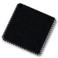
AD9255BCPZ-80 Analog Devices Inc, AD9255BCPZ-80 Datasheet - Page 8

AD9255BCPZ-80
Manufacturer Part Number
AD9255BCPZ-80
Description
IC ADC 14BIT 80MSPS 48LFCSP
Manufacturer
Analog Devices Inc
Datasheet
1.AD9255BCPZRL7-80.pdf
(44 pages)
Specifications of AD9255BCPZ-80
Data Interface
Serial, SPI™
Number Of Bits
14
Sampling Rate (per Second)
80M
Number Of Converters
1
Power Dissipation (max)
248mW
Voltage Supply Source
Analog and Digital
Operating Temperature
-40°C ~ 85°C
Mounting Type
Surface Mount
Package / Case
48-VFQFN, CSP Exposed Pad
Resolution (bits)
14bit
Sampling Rate
80MSPS
Input Channel Type
Differential
Supply Voltage Range - Analog
1.7V To 1.9V
Supply Voltage Range - Digital
1.7V To 1.9V
Lead Free Status / RoHS Status
Lead free / RoHS Compliant
Available stocks
Company
Part Number
Manufacturer
Quantity
Price
Company:
Part Number:
AD9255BCPZ-80
Manufacturer:
IXYS
Quantity:
2 300
Part Number:
AD9255BCPZ-80
Manufacturer:
ADI/亚德诺
Quantity:
20 000
AD9255
SWITCHING SPECIFICATIONS
AVDD = 1.8 V, DRVDD = 1.8 V, SVDD = 1.8 V, maximum sample rate, VIN = −1.0 dBFS differential input, 1.0 V internal reference, and
DCS enabled, unless otherwise noted.
Table 4.
Parameter
CLOCK INPUT PARAMETERS
DATA OUTPUT PARAMETERS
OUT-OF-RANGE RECOVERY TIME
1
2
3
4
5
The suffix following the part number refers to the model found in the
Conversion rate is the clock rate after the divider.
See the
Additional DCO delay can be added by writing to Bit 0 through Bit 4 in SPI Register 0x17 (see
Wake-up time is defined as the time required to return to normal operation from power-down mode.
Input Clock Rate
Conversion Rate
CLK Period—Divide-by-1 Mode (t
CLK Pulse Width High (t
Aperture Delay (t
Aperture Uncertainty (Jitter, t
CMOS Mode
LVDS Mode
Wake-Up Time
Divide-by-1 Mode
Data Propagation Delay (t
DCO Propagation Delay (t
Pipeline Delay (Latency)
DCO to Data Skew (t
Pipeline Delay (Latency)
DCS Enabled
DCS Disabled
Divide-by-3 Mode, Divide-by-5 Mode, and
Divide-by-2 Mode, Divide-by-4 Mode, Divide-
DCO to Data Skew (t
Data Propagation Delay (t
DCO Propagation Delay (t
DCS Enabled
DCS Disabled
Divide-by-7 Mode, DCS Enabled
by-6 Mode, and Divide-by-8 Mode, DCS
Input Clock Divider
Enabled or DCS Disabled
5
2
A
)
section for additional information on using the DCS with the input clock divider.
SKEW
SKEW
CH
)
)
)
DCO
PD
PD
DCO
J
)
)
)
)
)
3
4
CLK
4
)
3
Temp
Full
Full
Full
Full
Full
Full
Full
Full
Full
Full
Full
Full
Full
Full
Full
Full
Full
Full
Ordering Guide
Rev. A | Page 8 of 44
Min
20
10
12.5
3.75
5.9
0.8
0.8
2.4
2.7
0.3
2.6
3.3
−0.3
AD9255BCPZ-80
Typ
6.25
6.25
1.0
0.07
2.8
3.4
0.6
12
3.4
3.8
+0.4
12.5
500
2
section.
Table 17
Max
3.4
4.2
4.3
+1.2
625
80
80
8.75
6.6
0.9
4.2
1
).
Min
20
10
9.5
2.85
4.5
0.8
0.8
2.4
2.7
0.3
2.6
3.3
−0.3
AD9255BCPZ-105
Typ
4.75
4.75
1.0
0.07
2.8
3.4
0.6
12
3.4
3.8
+0.4
12.5
500
2
Max
625
105
105
6.65
5.0
3.4
4.2
0.9
4.2
4.3
+1.2
1
Min
20
10
8
2.4
3.8
0.8
0.8
2.4
2.7
0.3
2.6
3.3
−0.3
AD9255BCPZ-125
Typ
4
4
1.0
0.07
2.8
3.4
0.6
12
3.4
3.8
+0.4
12.5
500
2
+1.2
Max
625
125
125
5.6
4.2
3.4
4.2
0.9
4.2
4.3
1
Unit
MHz
MSPS
MSPS
ns
ns
ns
ns
ns
ns
ps rms
ns
ns
ns
Cycles
ns
ns
Cycles
μs
Cycles


