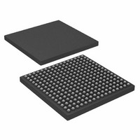
AD6654BBC Analog Devices Inc, AD6654BBC Datasheet - Page 74

AD6654BBC
Manufacturer Part Number
AD6654BBC
Description
IC ADC 14BIT W/6CH RSP 256CSPBGA
Manufacturer
Analog Devices Inc
Datasheet
1.AD6654CBCZ.pdf
(88 pages)
Specifications of AD6654BBC
Number Of Bits
14
Sampling Rate (per Second)
92.16M
Data Interface
Serial, Parallel
Number Of Converters
1
Power Dissipation (max)
2.5W
Voltage Supply Source
Analog and Digital
Operating Temperature
-25°C ~ 85°C
Mounting Type
Surface Mount
Package / Case
256-CSPBGA
Lead Free Status / RoHS Status
Contains lead / RoHS non-compliant
Available stocks
Company
Part Number
Manufacturer
Quantity
Price
Company:
Part Number:
AD6654BBC
Manufacturer:
AD
Quantity:
13 888
Company:
Part Number:
AD6654BBC
Manufacturer:
ADI
Quantity:
280
Company:
Part Number:
AD6654BBC
Manufacturer:
Analog Devices Inc
Quantity:
10 000
Part Number:
AD6654BBC
Manufacturer:
ADI/亚德诺
Quantity:
20 000
Company:
Part Number:
AD6654BBCZ
Manufacturer:
ADI
Quantity:
853
Company:
Part Number:
AD6654BBCZ
Manufacturer:
Analog Devices Inc
Quantity:
10 000
AD6654
GLOBAL REGISTER MAP
Chip I/O Access Control Register <7:0>
<7>: Synchronous Microport Bit. When this bit is set, the
microport assumes that its control signals (such as R/ W , DS ,
and CS ,) are synchronous to the CPUCLK. When cleared,
asynchronous control signals are assumed, and the microport
control signals are resynchronized with CPUCLK inside the
AD6654 part. Synchronous microport (when bit is set) has the
advantage of requiring a fewer number of clock cycles for
read/write access.
<6>: This bit is open.
<5:2>: Chip ID Bits. The chip ID bits are used to compare
against the chip ID input pins (CHIPID), enabling or disabling
I/O access for this specific chip. When more than one AD6654
part is sharing the microport, different CHIPID pins can be
used to differentiate among the parts. A particular part gives
I/O access only when the CHIPID pins have the same value as
these chip ID bits.
<1>: This bit is open.
<0>: Byte Mode Bit. The byte mode bit selects the bit width for
the microport operation. Table 29 shows details.
Table 29. Microport Data Bus Width Selection
Chip Access Control
Register <0>
0 (default)
1
Channel I/O Access Control Register <5:0>
These bits enable/disable the channel I/O access capability.
<5>: Channel 5 Access Bit. When the Channel 5 access bit is set
to Logic 1, any I/O write operation (from either the microport
or the serial port) that addresses a register located within the
channel register map updates the Channel 5 registers. Similarly,
for a read operation, the contents of the desired address in the
channel register map are output when this bit is set to Logic 1.
<4>: Channel 4 Access Bit. Similar to Bit <5> for Channel 4.
<3>: Channel 3 Access Bit. Similar to Bit <5> for Channel 3.
<2>: Channel 2 Access Bit. Similar to Bit <5> for Channel 2.
<1>: Channel 1 Access Bit. Similar to Bit <5> for Channel 1.
<0>: Channel 0 Access Bit. Similar to Bit <5> for Channel 0.
Note: If the access bits are set for more than one channel, during
write access all channels with access are written with the same
data. This is especially useful when more than one channel has
similar configurations. During a read operation, if more than
Microport Data Bus Bit Width
8-bit mode, using D <7:0>
16-bit mode, using D <15:0>
Rev. 0 | Page 74 of 88
one channel has access, the read access is given to the channel
with the lowest channel number.
For example, if both Channel 4 and Channel 2 have access bits
set, then read access is given to Channel 2.
Channel Enable Register <5:0>
<5>: Channel 5 Enable Bit. When this bit is set, Channel 5 logic
is enabled. When this bit is cleared, Channel 5 is disabled and
the channel’s logic does not consume any power. On power-up,
this bit comes up with Logic 0 and the channel is disabled. A
start sync does not start Channel 5, unless this bit is set before
issuing the start sync.
<4>: Channel 4 Enable Bit. Similar to Bit <5> for Channel 4.
<3>: Channel 3 Enable Bit. Similar to Bit <5> for Channel 3.
<2>: Channel 2 Enable Bit. Similar to Bit <5> for Channel 2.
<1>: Channel 1 Enable Bit. Similar to Bit <5> for Channel 1.
<0>: Channel 0 Enable Bit. Similar to Bit <5> for Channel 0.
Pin Synchronization Configuration <7:0>
<7>: Hop Synchronization Enable Bit. This bit is a global enable
for any hop synchronization involving SYNC pins. When this
bit is set, hop synchronization is enabled for all channels that
are programmed for pin synchronization. When this bit is
cleared, hop synchronization is not performed for any channel
that is programmed for pin synchronization.
<6>: Start Synchronization Enable Bit. This bit is a global enable
for any start synchronization involving SYNC pins. When this
bit is set, start synchronization is enabled for all channels that
are programmed for pin synchronization. When this bit is
cleared, start synchronization is not performed for any channel
that is programmed for pin synchronization.
<5>: First Sync Only Bit. When this bit is set, the NCO synchro-
nization logic recognizes only the first synchronization event as
valid. All other requests for synchronization events are ignored
as long as this bit is set. When cleared, all synchronization
events are acted upon.
<4>: Edge-Sensitivity Bit. When this bit is set, the rising edge on
the SYNC pin(s) is detected as a synchronization event (edge-
sensitive detection). When cleared, Logic 1 on the SYNC pin(s)
is detected as a synchronization event (level-sensitive
detection).
<3>: Enable Synchronization from SYNC3 Bit. When this bit is
set, the SYNC3 pin can be used for synchronization. When this
bit is cleared, the SYNC3 pin is ignored. This is a global enable
for all SYNC pins, and each individual channel selects which
pin it listens to.


