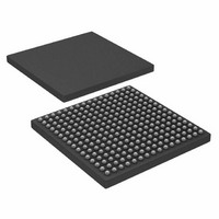
AD6654BBC Analog Devices Inc, AD6654BBC Datasheet - Page 76

AD6654BBC
Manufacturer Part Number
AD6654BBC
Description
IC ADC 14BIT W/6CH RSP 256CSPBGA
Manufacturer
Analog Devices Inc
Datasheet
1.AD6654CBCZ.pdf
(88 pages)
Specifications of AD6654BBC
Number Of Bits
14
Sampling Rate (per Second)
92.16M
Data Interface
Serial, Parallel
Number Of Converters
1
Power Dissipation (max)
2.5W
Voltage Supply Source
Analog and Digital
Operating Temperature
-25°C ~ 85°C
Mounting Type
Surface Mount
Package / Case
256-CSPBGA
Lead Free Status / RoHS Status
Contains lead / RoHS non-compliant
Available stocks
Company
Part Number
Manufacturer
Quantity
Price
Company:
Part Number:
AD6654BBC
Manufacturer:
AD
Quantity:
13 888
Company:
Part Number:
AD6654BBC
Manufacturer:
ADI
Quantity:
280
Company:
Part Number:
AD6654BBC
Manufacturer:
Analog Devices Inc
Quantity:
10 000
Part Number:
AD6654BBC
Manufacturer:
ADI/亚德诺
Quantity:
20 000
Company:
Part Number:
AD6654BBCZ
Manufacturer:
ADI
Quantity:
853
Company:
Part Number:
AD6654BBCZ
Manufacturer:
Analog Devices Inc
Quantity:
10 000
AD6654
Interrupt Enable Register <15:0>
<15>: AGC5 RSSI Update Enable Bit. When this bit is set, the
AGC5 RSSI update interrupt is enabled, allowing an interrupt
to be generated when the RSSI word is updated.
When this bit is cleared, an interrupt cannot be generated for
this event. Also, see the Interrupt Status Register <15:0> section.
<14>: AGC4 RSSI Update Enable Bit. Similar to Bit <15> for
the AGC4.
<13>: AGC3 RSSI Update Enable Bit. Similar to Bit <15> for
the AGC3.
<12>: AGC2 RSSI Update Enable Bit. Similar to Bit <15> for
the AGC2.
<11>: AGC1 RSSI Update Enable Bit. Similar to Bit <15> for
the AGC1.
<10>: AGC0 RSSI Update Enable Bit. Similar to Bit <15> for
the AGC0.
<9>: Channel 5 Data Ready Enable Bit. When this bit is set, the
Channel 5 data ready interrupt is enabled, allowing an interrupt
to be generated when Channel 5 BIST signature registers are
updated. When this bit is cleared, an interrupt cannot be
generated for this event.
<8>: Channel 4 Data Ready Enable Bit. Similar to Bit <9> for
Channel 4.
<7>: Channel 3 Data Ready Enable Bit. Similar to Bit <9> for
Channel 3.
<6>: Channel 2 Data Ready Enable Bit. Similar to Bit <9> for
Channel 2.
<5>: Channel 1 Data Ready Enable Bit. Similar to Bit <9> for
Channel 1.
<4>: Channel 0 Data Ready Enable Bit. Similar to Bit <9> for
Channel 0.
<3>: Reserved. This bit must be written with Logic 0.
<2>: ADC Port Power Monitoring Enable Bit. When this bit is
set to Logic 1, the ADC port power monitoring interrupt is
enabled, allowing an interrupt to be generated when ADC port
power monitoring registers are updated. When set to Logic 1,
the ADC port power monitoring interrupt is disabled.
<1>: Reserved. This bit must be written with Logic 0.
<0>: Reserved. This bit must be written with Logic 0.
Rev. 0 | Page 76 of 88
INPUT PORT REGISTER MAP
ADC Input Control Register <27:0>
These bits are general control bits for the ADC input logic.
<27>: PN Active Bit. When this bit is set, the pseudorandom
number generator is active. When this bit is cleared, the PN
generator is disabled and the seed is set to its default value.
<26>: EXP Lock Bit. When this bit is set along with the PN
active bit, then the EXP signal for pseudorandom input is
locked to 000 (giving full-scale input). When this bit is cleared,
EXP bits for pseudorandom input are randomly generated input
data bits.
<25> Reserved. This bit must be written with Logic 0.
<24> Reserved. This bit must be written with Logic 0.
<23:20>: Channel 5 Cross Bar Mux Select Bits. These bits select
the source of input data for Channel 5. See Table 30.
Table 30. Input Data Source Selection
Cross Bar Mux Select Bits
0010
0100
<19>: Reserved. This bit must be written with Logic 0.
<18:16>: Channel 4 Cross Bar Mux Select Bits. Similar to bits
<22:20>, but for Channel 4.
<15>: Reserved. This bit must be written with Logic 0.
<14:12>: Channel 3 Cross Bar Mux Select Bits. Similar to
Bits <22:20> for Channel 3.
<11>: Reserved. This bit must be written with Logic 0.
<10:8>: Channel 2 Cross Bar Mux Select Bits. Similar to
Bits <22:20> for Channel 2.
<7>: Reserved. This bit must be written with Logic 0.
<6:4>: Channel 1 Cross Bar Mux Select Bits. Similar to
Bits <22:20> for Channel 1.
<3>: Reserved. This bit must be written with Logic 0.
<2:0>: Channel 0 Cross Bar Mux Select Bits. Similar to
Bits <22:20> for Channel 0.
ADC CLK Control Register <11:0>.
These bits control the ADC clocks and internal PLL clock.
<11>: Reserved. This bit must be written with Logic 0.
Configuration
ADC port drives input (real)
PN sequence drives input (real)


