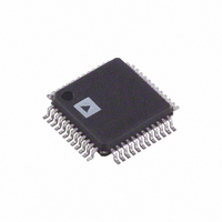
AD9244BST-40 Analog Devices Inc, AD9244BST-40 Datasheet - Page 21

AD9244BST-40
Manufacturer Part Number
AD9244BST-40
Description
IC ADC 14BIT 40MSPS 48-LQFP
Manufacturer
Analog Devices Inc
Datasheet
1.AD9244BSTZ-65.pdf
(36 pages)
Specifications of AD9244BST-40
Rohs Status
RoHS non-compliant
Number Of Bits
14
Sampling Rate (per Second)
40M
Data Interface
Parallel
Number Of Converters
1
Power Dissipation (max)
300mW
Voltage Supply Source
Analog and Digital
Operating Temperature
-40°C ~ 85°C
Mounting Type
Surface Mount
Package / Case
48-LQFP
For Use With
AD9244-65PCBZ - BOARD EVAL FOR AD9244-65AD9244-40PCBZ - BOARD EVAL FOR AD9244-40
Available stocks
Company
Part Number
Manufacturer
Quantity
Price
Company:
Part Number:
AD9244BST-40
Manufacturer:
ADI
Quantity:
210
Part Number:
AD9244BST-40
Manufacturer:
ADI/亚德诺
Quantity:
20 000
Using an External Reference
To use an external reference, the internal reference must be dis-
abled by connecting the SENSE pin to AVDD. The AD9244
contains an internal reference buffer, A2 (see Figure 48), that
simplifies the drive requirements of an external reference. The
external reference must be able to drive a 5 kΩ (±20%) load.
The bandwidth of the reference is deliberately left small to
minimize the reference noise contribution. As a result, it is not
possible to drive VREF externally with high frequencies.
Figure 51 shows an example of an external reference driving
both VIN– and VREF. In this case, both the common-mode
voltage and input span are directly dependent on the value of
VREF. Both the input span and the center of the input span are
equal to the external VREF. Thus, the valid input range extends
from (VREF + VREF/2) to (VREF − VREF/2). For example, if
the Precision Reference Part REF191, a 2.048 V external refer-
ence, is used, the input span is 2.048 V. In this case, 1 LSB of the
AD9244 corresponds to 0.125 mV.
It is essential that a minimum of a 10 μF capacitor, in parallel
with a 0.1 μF low inductance ceramic capacitor, decouple the
reference output to AGND.
DIGITAL INPUTS AND OUTPUTS
Table 10. Output Data Format
Input (V)
VIN+ – VIN−
VIN+ – VIN−
VIN+ – VIN−
VIN+ – VIN−
VIN+ – VIN−
5V
0.1μF
VREF + VREF/2
VREF – VREF/2
VREF
Figure 51. Using an External Reference
AVDD
10μF
+
0.1μF
Condition (V)
< –VREF/2 − 0.5 LSB
= −VREF/2
= 0
= +VREF/2 − 1.0 LSB
> +VREF/2 − 0.5 LSB
20pF
33Ω
33Ω
VIN+
VIN–
VREF
SENSE
AD9244
REFB
REFT
0.1μF
0.1μF
0.1μF
Binary Output Mode
00 0000 0000 0000
00 0000 0000 0000
10 0000 0000 0000
11 1111 1111 1111
11 1111 1111 1111
+
10μF
Rev. C | Page 21 of 36
Digital Outputs
Table 10 details the relationship among the ADC input, OTR,
and digital output format.
Data Format Select (DFS)
The AD9244 can be programmed for straight binary or twos
complement data on the digital outputs. Connect the DFS pin to
AGND for straight binary and to AVDD for twos complement.
Digital Output Driver Considerations
The AD9244 output drivers can be configured to interface with
5 V or 3.3 V logic families by setting DRVDD to 5 V or 3.3 V,
respectively. The output drivers are sized to provide sufficient
output current to drive a wide variety of logic families.
However, large drive currents tend to cause glitches on the
supplies and can affect converter performance. Applications
requiring the ADC to drive large capacitive loads or large
fanouts can require external buffers or latches.
Twos Complement Mode
10 0000 0000 0000
10 0000 0000 0000
00 0000 0000 0000
01 1111 1111 1111
01 1111 1111 1111
OTR
1
0
0
0
1
AD9244


