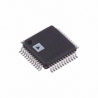
AD9244BST-40 Analog Devices Inc, AD9244BST-40 Datasheet - Page 24

AD9244BST-40
Manufacturer Part Number
AD9244BST-40
Description
IC ADC 14BIT 40MSPS 48-LQFP
Manufacturer
Analog Devices Inc
Datasheet
1.AD9244BSTZ-65.pdf
(36 pages)
Specifications of AD9244BST-40
Rohs Status
RoHS non-compliant
Number Of Bits
14
Sampling Rate (per Second)
40M
Data Interface
Parallel
Number Of Converters
1
Power Dissipation (max)
300mW
Voltage Supply Source
Analog and Digital
Operating Temperature
-40°C ~ 85°C
Mounting Type
Surface Mount
Package / Case
48-LQFP
For Use With
AD9244-65PCBZ - BOARD EVAL FOR AD9244-65AD9244-40PCBZ - BOARD EVAL FOR AD9244-40
Available stocks
Company
Part Number
Manufacturer
Quantity
Price
Company:
Part Number:
AD9244BST-40
Manufacturer:
ADI
Quantity:
210
Part Number:
AD9244BST-40
Manufacturer:
ADI/亚德诺
Quantity:
20 000
AD9244
Clock Stabilizer (DCS)
The clock stabilizer circuit in the AD9244 desensitizes the ADC
from clock duty cycle variations. System clock constraints are
eased by internally restoring the clock duty cycle to 50%,
independent of the clock input duty cycle. Low jitter on the
rising edge (sampling edge) of the clock is preserved while the
falling edge is generated on-chip.
It may be desirable to disable the clock stabilizer, or necessary
when the clock frequency is varied or completely stopped. Note
that stopping the clock is not recommended with ac-coupled
clocks. Once the clock frequency is changed, more than 100
clock cycles may be required for the clock stabilizer to settle to
the new speed. When the stabilizer is disabled, the internal
switching is directly affected by the clock state. If CLK+ is high,
the SHA is in hold mode; if CLK+ is low, the SHA is in track
mode. Figure 25 shows the benefits of using the clock stabilizer.
Connecting DCS to AVDD implements the internal clock
stabilization function in the AD9244. If the DCS pin is
connected to ground, the AD9244 uses both edges of the
external clock in its internal timing circuitry (see the
Specifications section for timing requirements).
Grounding and Decoupling
Analog and Digital Grounding
Proper grounding is essential in high speed, high resolution
systems. Multilayer printed circuit boards (PCBs) are recom-
mended to provide optimal grounding and power distribution.
The use of power and ground planes offers distinct advantages,
including:
•
•
•
It is important to design a layout that minimizes noise from
coupling onto the input signal. Digital input signals should not
be run in parallel with input signal traces and should be routed
away from the input circuitry. While the AD9244 features sepa-
rate analog and digital ground pins, it should be treated as an
analog component. The AGND and DGND pins must be joined
together directly under the AD9244. A solid ground plane
under the ADC is acceptable if the power and ground return
currents are carefully managed.
The minimization of the loop area encompassed by a signal
and its return path
The minimization of the impedance associated with ground
and power paths
The inherent distributed capacitor formed by the power
plane, PCB material, and ground plane
Rev. C | Page 24 of 36
Analog Supply Decoupling
The AD9244 features separate analog and digital supply and
ground circuits, helping to minimize digital corruption of
sensitive analog signals. In general, AVDD (analog power)
should be decoupled to AGND (analog ground). The AVDD
and AGND pins are adjacent to one another. Figure 61 shows
the recommended decoupling for each pair of analog supplies;
0.1 μF ceramic chip and 10 μF tantalum capacitors should pro-
vide adequately low impedance over a wide frequency range.
The decoupling capacitors (especially 0.1 μF) should be located
as close to the pins as possible.
Digital Supply Decoupling
The digital activity on the AD9244 falls into two categories:
correction logic and output drivers. The internal correction
logic draws relatively small surges of current, mainly during
the clock transitions. The output drivers draw large current
impulses when the output bits change state. The size and
duration of these currents are a function of the load on the
output bits; large capacitive loads should be avoided.
For the digital decoupling shown in Figure 62, 0.1 μF ceramic
chip and 10 μF tantalum capacitors are appropriate. The
decoupling capacitors (especially 0.1 μF) should be located as
close to the pins as possible. Reasonable capacitive loads on the
data pins are less than 20 pF per bit. Applications involving
greater digital loads should consider increasing the digital
decoupling and/or using external buffers/latches.
A complete decoupling scheme also includes large tantalum or
electrolytic capacitors on the power supply connector to reduce
low frequency ripple to insignificant levels.
10μF
1
10μF
1
LOCATE AS CLOSE AS POSSIBLE TO SUPPLY PINS.
LOCATE AS CLOSE AS POSSIBLE TO SUPPLY PINS.
+
+
Figure 61. Analog Supply Decoupling
Figure 62. Digital Supply Decoupling
0.1μF
0.1μF
1
1
AVDD
AGND
DRVDD
DGND
AD9244
AD9244


