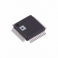
AD7653AST Analog Devices Inc, AD7653AST Datasheet - Page 21

AD7653AST
Manufacturer Part Number
AD7653AST
Description
IC ADC 16BIT 1MSPS W/REF 48-LQFP
Manufacturer
Analog Devices Inc
Series
PulSAR®r
Datasheet
1.AD7653ASTZ.pdf
(28 pages)
Specifications of AD7653AST
Rohs Status
RoHS non-compliant
Number Of Bits
16
Sampling Rate (per Second)
1M
Data Interface
Serial, Parallel
Number Of Converters
1
Power Dissipation (max)
145mW
Voltage Supply Source
Analog and Digital
Operating Temperature
-40°C ~ 85°C
Mounting Type
Surface Mount
Package / Case
48-LQFP
For Use With
EVAL-AD7653CBZ - BOARD EVALUATION FOR AD7653
Available stocks
Company
Part Number
Manufacturer
Quantity
Price
Company:
Part Number:
AD7653ASTZ
Manufacturer:
ADI
Quantity:
274
Company:
Part Number:
AD7653ASTZ
Manufacturer:
Analog Devices Inc
Quantity:
10 000
Company:
Part Number:
AD7653ASTZRL
Manufacturer:
Analog Devices Inc
Quantity:
10 000
MASTER SERIAL INTERFACE
Internal Clock
The AD7653 is configured to generate and provide the serial
data clock SCLK when the EXT/ INT pin is held LOW. The
AD7653 also generates a SYNC signal to indicate to the host
when the serial data is valid. The serial clock SCLK and the
SYNC signal can be inverted, if desired. Depending on the
RDC/SDIN input, the data can be read after each conversion or
during the following conversion. F
the detailed timing diagrams of these two modes.
CS, RD
CS, RD
SDOUT
CNVST
SDOUT
CNVST
BUSY
SYNC
SCLK
BUSY
SYNC
SCLK
t
16
t
3
Figure 33. Master Serial Data Timing for Reading (Read Previous Conversion during Convert)
igure 32
t
t
t
14
15
16
t
t
t
14
15
29
t
17
X
t
t
Figure 32. Master Serial Data Timing for Reading (Read after Convert)
18
22
and
EXT/INT = 0
t
EXT/INT = 0
1
Figure 33
t
D15
3
X
t
t
1
20
22
t
19
t
21
t
20
D14
t
D15
2
23
show
1
t
19
t
Rev. A | Page 21 of 28
18
RDC/SDIN = 0
RDC/SDIN = 1
D14
t
t
21
2
3
23
t
28
3
Usually, because the AD7653 is used with a fast throughput, the
Master Read During Conversion mode is the most
recommended serial mode. In this mode, the serial clock and
data toggle at appropriate instants, minimizing potential
feedthrough between digital activity and critical conversion
decisions.
In Read After Conversion mode, it should be noted that unlike
in other modes, the BUSY signal returns LOW after the 16 data
bits are pulsed out and not at the end of the conversion phase,
which results in a longer BUSY width.
INVSCLK = INVSYNC = 0
14
D2
INVSCLK = INVSYNC = 0
14
D2
15
D1
15
D1
16
t
24
16
t
30
D0
t
D0
24
02966-0-015
02966-0-016
t
t
t
t
t
t
25
26
27
25
26
27
AD7653


