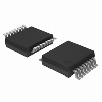
UDA1361TS/N1,112 NXP Semiconductors, UDA1361TS/N1,112 Datasheet - Page 6

UDA1361TS/N1,112
Manufacturer Part Number
UDA1361TS/N1,112
Description
IC ADC STEREO AUDIO 24BIT 16SSOP
Manufacturer
NXP Semiconductors
Type
Stereo Audior
Datasheet
1.UDA1361TSN1118.pdf
(18 pages)
Specifications of UDA1361TS/N1,112
Package / Case
16-SSOP
Resolution (bits)
24 b
Sampling Rate (per Second)
110k
Data Interface
Serial
Voltage Supply Source
Analog and Digital
Voltage - Supply
2.4 V ~ 3.6 V
Operating Temperature
-40°C ~ 85°C
Mounting Type
Surface Mount
Resolution
24 bit
Operating Supply Voltage
2.4 V to 3.6 V
Mounting Style
SMD/SMT
Operating Temperature Range
- 40 C to + 85 C
Supply Current
10.5 mA
Lead Free Status / RoHS Status
Lead free / RoHS Compliant
Lead Free Status / RoHS Status
Lead free / RoHS Compliant, Lead free / RoHS Compliant
Other names
568-1158-5
935267099112
UDA1361TSDK
935267099112
UDA1361TSDK
Available stocks
Company
Part Number
Manufacturer
Quantity
Price
Company:
Part Number:
UDA1361TS/N1,112
Manufacturer:
MICROCHIP
Quantity:
85
NXP Semiconductors
Table 4 Decimation filter characteristic
DC cancellation filter
A IIR high-pass filter is provided to remove unwanted
DC components. The filter characteristics are given in
Table 5.
Table 5 DC cancellation filter characteristic
Serial interface formats
2002 Nov 25
handbook, full pagewidth
Pass-band ripple 0 to 0.45f
Pass-band droop 0.45f
Stop band
Dynamic range
Pass-band ripple −
Pass-band gain
Droop
Attenuation
at DC
Dynamic range
96 kHz sampling 24-bit stereo audio ADC
ITEM
ITEM
DATA
DATA
BCK
BCK
WS
WS
MSB
1
1
>0.55 f
0 to 0.45 f
−
at 0.00045f
at 0.00000036f
0 to 0.45f
MSB
B2
CONDITION
CONDITION
2
2
s
LEFT
LEFT
B2
s
3
3
s
s
s
s
s
±0.01
−0.2
−70
>135
none
0
−0.031
>40
>135
VALUE (dB)
VALUE (dB)
Fig.3 Serial interface formats.
MSB-JUSTIFIED FORMAT
INPUT FORMAT I
LSB
≥8
≥8
MSB
LSB
6
1
1
Mute
On recovery from Power-down, the serial data output
DATAO is held LOW until valid data is available from the
decimation filter. This time tracks with the sampling
frequency:
Power-down mode/input voltage control
The PWON pin can control the power saving together with
the optional gain switch for 2 or 1 V (RMS) input.
The UDA1361TS supports 2 V (RMS) input using a series
resistor of 12 kΩ. For the definition of the pin settings for
1 or 2 V (RMS) mode, it is assumed that this resistor is
present as a default component.
Table 6 Power-down/input voltage control
t
MSB
2
=
B2
S-BUS
2
2
12288
--------------- -
RIGHT
RIGHT
f
B2
s
3
3
PWON
, t = 256 ms when f
M
H
L
Power-down mode
0 dB gain
6 dB gain
POWER-DOWN OR GAIN
s
= 48 kHz.
LSB
≥8
≥8
UDA1361TS
Product specification
MSB
LSB
MGT453
MSB
B2


