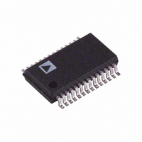
AD974ARS Analog Devices Inc, AD974ARS Datasheet

AD974ARS
Specifications of AD974ARS
Available stocks
Related parts for AD974ARS
AD974ARS Summary of contents
Page 1
FEATURES Fast 16-Bit ADC with 200 kSPS Throughput Four Single-Ended Analog Input Channels Single +5 V Supply Operation Input Ranges and 120 mW Max Power Dissipation Power-Down Mode 50 ...
Page 2
AD974–SPECIFICATIONS Parameter RESOLUTION ANALOG INPUT Voltage Range Impedance Sampling Capacitance THROUGHPUT SPEED Complete Cycle (Acquire and Convert) Throughput Rate DC ACCURACY Integral Linearity Error Differential Linearity Error No Missing Codes 2 Transition Noise 3 Full-Scale Error Full-Scale Error Drift Full-Scale ...
Page 3
Parameter Conditions DIGITAL OUTPUTS Data Format Data Coding SINK SOURCE Output Capacitance High-Z State Leakage Current High-Z State V OUT POWER SUPPLIES Specified Performance V DIG V ANA I DIG I ANA Power Dissipation ...
Page 4
... C to +85 C AD974BN – +85 C AD974AR – +85 C AD974BR – +85 C AD974ARS – +85 C AD974BRS – +85 C CAUTION ESD (electrostatic discharge) sensitive device. Electrostatic charges as high as 4000 V readily accumulate on the human body and test equipment and can discharge without detection. Although the AD974 features proprietary ESD protection circuitry, permanent damage may occur on devices subjected to high energy electrostatic discharges ...
Page 5
Pin No. Mnemonic Description 1 AGND1 Analog Ground. Used as the ground reference point for the REF pin. 2–5, 25–28 VxA, VxB Analog Input. Refer to Table I for input range configuration. 6 BIP Bipolar Offset. Connect VxA inputs to ...
Page 6
AD974 DEFINITION OF SPECIFICATIONS INTEGRAL NONLINEARITY ERROR (INL) Linearity error refers to the deviation of each individual code from a line drawn from “negative full scale” through “positive full scale.” The point used as “negative full scale” occurs 1/2 LSB ...
Page 7
CONVERSION CONTROL The AD974 is controlled by two signals: R/C and CS. When R/C is brought low, with CS low, for a minimum of 50 ns, the input signal will be held on the internal capacitor array and a conversion ...
Page 8
AD974 can be read after the conversion is complete. The external clock can be either a continuous or discontinuous clock. A discontinu- ous clock can be either normally low or normally high when inactive. In the case of the discontinuous ...
Page 9
EXTERNAL DISCONTINUOUS CLOCK DATA READ DURING CONVERSION WITH NO SYNC OUTPUT GENERATED Figure 5 illustrates the method by which data from conversion “n-1” can be read during conversion “n” while using a discon- tinuous external clock, without the generation of ...
Page 10
AD974 EXTERNAL DISCONTINUOUS CLOCK DATA READ DURING CONVERSION WITH SYNC OUTPUT GENERATED Figure 7 illustrates the method by which data from conversion “n-1” can be read during conversion “n” while using a discon- tinuous external clock, with the generation of ...
Page 11
EXTERNAL CONTINUOUS CLOCK DATA READ AFTER CONVERSION WITH SYNC OUTPUT GENERATED Figure 8 illustrates the method by which data from conversion “n” can be read after the conversion is complete using a con- tinuous external clock, with the generation of ...
Page 12
AD974 EXTERNAL CONTINUOUS CLOCK DATA READ DURING CONVERSION WITH SYNC OUTPUT GENERATED Figure 9 illustrates the method by which data from conversion “n-1” can be read during conversion “n” while using a continu- ous external clock with the generation of ...
Page 13
Input Voltage Range Description Full-Scale Range Least Significant Bit +Full Scale (FS – 1 LSB) Midscale One LSB Below Midscale –Full Scale ANALOG INPUTS The AD974 is specified ...
Page 14
AD974 INPUT RANGE BASIC CONNECTIONS FOR AD974 BIP VxA V VxB IN AGND1 10V CAP + 2.2 F AD974 REF + 2.2 F AGND2 BIP V VxA IN VxB AGND1 0V TO +5V CAP + 2.2 F AD974 REF + ...
Page 15
OFFSET AND GAIN ADJUSTMENT The AD974 is factory trimmed to minimize gain, offset and linearity errors. There are no internal provisions to allow for any further adjustment of offset error through external circuitry. The reference of the AD974 can be ...
Page 16
AD974 AC PERFORMANCE The AD974 is fully specified and tested for dynamic perfor- mance specifications. The ac parameters are required for signal processing applications such as speech recognition and spectrum analysis. These applications require information on the ADC’s effect on ...
Page 17
SFDR 105 100 95 THD 90 SNRD –75 –50 – TEMPERATURE – C Figure 20. AC Parameters vs. Temperature DC CODE UNCERTAINTY Ideally, a fixed dc input should result in the same output code ...
Page 18
AD974 0 –10 –20 –30 –40 –50 –60 –70 –80 –90 –100 –110 –120 –130 FREQUENCY – kHz Figure 24. Adjacent Channel Crosstalk, Worst Pair (8192 Point FFT; AIN 2 = 220 kHz, ...
Page 19
The AD974 may be operated from a single +5 V supply. When separate supplies are used, however beneficial to have larger (10 F) capacitors placed between the logic supply (V ) and digital common (DGND), and between the ...
Page 20
AD974 PIN 1 0.210 (5.33) MAX SEATING PLANE 28 1 0.0118 (0.30) 0.0040 (0.10) 0.078 (1.98) 0.068 (1.73) 0.008 (0.203) 0.002 (0.050) OUTLINE DIMENSIONS Dimensions shown in inches and (mm). 28-Lead 300 Mil Plastic DIP (N-28B) 1.425 (38.195) 1.385 (35.179) ...


