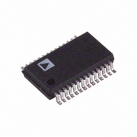
AD974ARS Analog Devices Inc, AD974ARS Datasheet - Page 13

AD974ARS
Manufacturer Part Number
AD974ARS
Description
IC DAS 16BIT 4CH 200KSPS 28-SSOP
Manufacturer
Analog Devices Inc
Type
Data Acquisition System (DAS)r
Datasheet
1.AD974ANZ.pdf
(20 pages)
Specifications of AD974ARS
Rohs Status
RoHS non-compliant
Resolution (bits)
16 b
Sampling Rate (per Second)
200k
Data Interface
Serial
Voltage Supply Source
Analog and Digital
Voltage - Supply
5V
Operating Temperature
-40°C ~ 85°C
Mounting Type
Surface Mount
Package / Case
28-SSOP
For Use With
EVAL-AD974CB - BOARD EVAL FOR AD974
Available stocks
Company
Part Number
Manufacturer
Quantity
Price
Part Number:
AD974ARS
Manufacturer:
ADI/亚德诺
Quantity:
20 000
Part Number:
AD974ARSZ
Manufacturer:
ADI/亚德诺
Quantity:
20 000
REV. A
Description
Full-Scale Range
Least Significant Bit
+Full Scale (FS – 1 LSB)
Midscale
One LSB Below Midscale
–Full Scale
ANALOG INPUTS
The AD974 is specified to operate with three full-scale analog
input ranges. Connections required for each of the eight analog
inputs, VxA and VxB and the resulting full-scale ranges, are
shown in Table I. The nominal input impedance for each ana-
log input range is also shown. Table II shows the output codes
for the ideal input voltages of each of the analog input ranges.
The analog input section has a 25 V overvoltage protection on
VxA and VxB. Since the AD974 has two analog grounds it is
important to ensure that the analog input is referenced to the
AGND1 pin, the low current ground. This will minimize any
problems associated with a resistive ground drop. It is also
important to ensure that the analog inputs are driven by a low
impedance source. With its primarily resistive analog input
circuitry, the ADC can be driven by a wide selection of general
purpose amplifiers.
To achieve the low distortion capability of the AD974 care
should be taken in the selection of the drive circuitry
op amp.
Input Voltage
Range
0 V to +5 V
0 V to +4 V
10 V
Table II. Output Codes and Ideal Input Voltage
305 V
0 V
–305 V
–10 V
+9.999695 V
10 V
Connect
VxA to
BIP
V
V
Table I. Analog Input Configuration
IN
IN
Analog Input
–13–
0 V to +5 V
76 V
+2.5 V
+2.499924 V
0 V
+4.999847 V
Figure 10 shows the simplified analog input section for the
AD974. Since the AD974 can operate with an internal or exter-
nal reference, and three different analog input ranges, the full-
scale analog input range is best represented with a voltage that
spans 0 V to V
chip resistors are laser trimmed to ratio match for adjustment of
offset and full-scale error using fixed external resistors.
Connect
VxB to
V
GND
V
IN
IN
AGND2
CAP
VxA
VxB
Figure 10. Simplified Analog Input
REF
12k
BIP
3k
4k
across the 40 pF sampling capacitor. The on-
0 V to +4 V
61 V
+3.999939 V
+2 V
+1.999939 V
0 V
AGND1
Input
Impedance
13.7 k
6.0 k
6.4 k
AD974
REF
4k
Digital Input
Straight Binary
1111 1111 1111 1111
1000 0000 0000 0000
0111 1111 1111 1111
0000 0000 0000 0000
SWITCHED
REFERENCE
CAP ADC
40pF
2.5V
AD974


