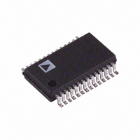
AD974ARS Analog Devices Inc, AD974ARS Datasheet - Page 19

AD974ARS
Manufacturer Part Number
AD974ARS
Description
IC DAS 16BIT 4CH 200KSPS 28-SSOP
Manufacturer
Analog Devices Inc
Type
Data Acquisition System (DAS)r
Datasheet
1.AD974ANZ.pdf
(20 pages)
Specifications of AD974ARS
Rohs Status
RoHS non-compliant
Resolution (bits)
16 b
Sampling Rate (per Second)
200k
Data Interface
Serial
Voltage Supply Source
Analog and Digital
Voltage - Supply
5V
Operating Temperature
-40°C ~ 85°C
Mounting Type
Surface Mount
Package / Case
28-SSOP
For Use With
EVAL-AD974CB - BOARD EVAL FOR AD974
Available stocks
Company
Part Number
Manufacturer
Quantity
Price
Part Number:
AD974ARS
Manufacturer:
ADI/亚德诺
Quantity:
20 000
Part Number:
AD974ARSZ
Manufacturer:
ADI/亚德诺
Quantity:
20 000
The AD974 may be operated from a single +5 V supply.
When separate supplies are used, however, it is beneficial to
have larger (10 F) capacitors placed between the logic supply
(V
supply (V
ally, 10 F capacitors should be located in the vicinity of the
ADC to further reduce low frequency ripple. In systems where
the device will be subjected to harsh environmental noise,
additional decoupling may be required.
GROUNDING
The AD974 has three ground pins; AGND1, AGND2 and
DGND. The analog ground pins are the “high quality” ground
reference points and should be connected to the system analog
common. AGND2 is the ground to which most internal ADC
analog signals are referenced. This ground is most susceptible to
current-induced voltage drops and thus must be connected with
the least resistance back to the power supply. AGND1 is the low
current analog supply ground and should be the analog common
for the external reference, input op amp drive circuitry and the
input resistor divider circuit. By applying the inputs referenced
to this ground, any ground variations will be offset and have a
minimal effect on the resulting analog input to the ADC. The
digital ground pin, DGND, is the reference point for all of the
digital signals that control the AD974.
The AD974 can be powered with two separate power supplies or
with a single analog supply. When the system digital supply is
noisy, or fast switching digital signals are present, it is recom-
mended to connect the analog supply to both the V
pins of the AD974 and the system supply to the remaining
digital circuitry. With this configuration, AGND1, AGND2 and
DGND should be connected back at the ADC. When there is
significant bus activity on the digital output pins, the digital and
analog supply pins on the ADC should be separated. This would
eliminate any high speed digital noise from coupling back to the
analog portion of the AD974. In this configuration, the digital
ground pin DGND should be connected to the system digital
ground and be separate from the AGND pins.
REV. A
DIG
) and digital common (DGND), and between the analog
ANA
) and the analog common (AGND2). Addition-
ANA
and V
DIG
–19–
BOARD LAYOUT
Designing with high resolution data converters requires careful
attention to board layout and trace impedance is a significant
issue. A 1.22 mA current through a 0.5
voltage drop of 0.6 mV, which is 2 LSBs at the 16-bit level over
the 20 volt full-scale range. Ground circuit impedances should
be reduced as much as possible since any ground potential
differences between the signal source and the ADC appear as
an error voltage in series with the input signal. In addition to
ground drops, inductive and capacitive coupling needs to be
considered. This is especially true when high accuracy analog
input signals share the same board with digital signals. Thus, to
minimize input noise coupling, the input signal leads to V
the signal return leads from AGND should be kept as short as
possible. In addition, power supplies should also be decoupled
to filter out ac noise.
Analog and digital signals should not share a common path.
Each signal should have an appropriate analog or digital return
routed close to it. Using this approach, signal loops enclose a
small area, minimizing the inductive coupling of noise. Wide
PC tracks, large gauge wire and ground planes are highly rec-
ommended to provide low impedance signal paths. Separate
analog and digital ground planes are also recommended with a
single interconnection point to minimize ground loops. Analog
signals should be routed as far as possible from high speed
digital signals and if absolutely necessary, should only cross
them at right angles.
In addition, it is recommended that multilayer PC boards be
used with separate power and ground planes. When designing
the separate sections, careful attention should be paid to the
layout.
trace will develop a
AD974
IN
and


