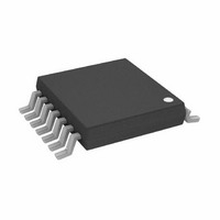
AD5293BRUZ-20 Analog Devices Inc, AD5293BRUZ-20 Datasheet - Page 19

AD5293BRUZ-20
Manufacturer Part Number
AD5293BRUZ-20
Description
IC DGTL POT 1024POS 20K 14TSSOP
Manufacturer
Analog Devices Inc
Datasheet
1.AD5293BRUZ-20.pdf
(24 pages)
Specifications of AD5293BRUZ-20
Temperature Coefficient
35 ppm/°C Typical
Taps
1024
Resistance (ohms)
20K
Number Of Circuits
1
Interface
SPI Serial
Voltage - Supply
9 V ~ 33 V, ±9 V ~ 16.5 V
Operating Temperature
-40°C ~ 105°C
Mounting Type
Surface Mount
Package / Case
14-TSSOP
Resistance In Ohms
20K
End To End Resistance
20kohm
Track Taper
Linear
No. Of Steps
256
Resistance Tolerance
± 1%
Control Interface
Serial, SPI
No. Of Pots
Single
Potentiometer Ic
RoHS Compliant
Supply Voltage Range
± 9V To ± 16.5V
Rohs Compliant
Yes
Lead Free Status / RoHS Status
Lead free / RoHS Compliant
Memory Type
-
Lead Free Status / RoHS Status
Lead free / RoHS Compliant
Other names
AD5293BRUZ-20-U1
AD5293BRUZ-20-U1
AD5293BRUZ-20-U1
Available stocks
Company
Part Number
Manufacturer
Quantity
Price
Company:
Part Number:
AD5293BRUZ-20
Manufacturer:
Analog Devices Inc
Quantity:
1 941
Part Number:
AD5293BRUZ-20
Manufacturer:
ADI/亚德诺
Quantity:
20 000
RESET
A low-to-high transition of the hardware RESET pin loads the
RDAC register with midscale. The AD5293 can also be reset
through software by executing Command 3 (see
The control register is restored with default bits (see
RESISTOR PERFORMANCE MODE
This mode activates a new, patented 1% end-to-end resistor
tolerance that ensures a ±1% resistor tolerance on each code,
that is, code = half scale, R
Table 4 to verify which codes achieve ±1% resistor tolerance.
The resistor performance mode is activated by programming
Bit C2 of the control register (see Table 12 and Table 13). The
typical settling time is shown in Figure 32.
SDO PIN AND DAISY-CHAIN OPERATION
The serial data output pin (SDO) serves two purposes: it can
be used to read the contents of the wiper setting and control
register using Command 2, and Command 5, respectively (see
Table 11) or the SDO pin can be used in daisy-chain mode.
Data is clocked out of SDO on the rising edge of SCLK. The
SDO pin contains an open-drain N-channel FET that requires
a pull-up resistor if this pin is used. To place the pin in high
impedance and minimize the power dissipation when the pin
is used, the 0x8001 data word followed by Command 0 should
be sent to the part. Table 10 provides a sample listing for the
Table 10. Minimize Power Dissipation at the SDO Pin
DIN
0xXXXX
0x8001
0x0000
1
Table 11. Command Operation Truth Table
Command
0
1
2
3
4
5
6
1
Table 12. Control Register Bit Map
D9
X
1
X = don’t care.
X = don’t care.
X = don’t care.
1
Command Bits[B13:B10]
C3
0
0
0
0
0
0
1
D8
X
1
C2
0
0
0
1
1
1
0
SDO
0xXXXX
0xXXXX
High impedance
1
WB
C1
0
0
1
0
1
1
0
D7
X
=10 kΩ ± 100 Ω. See Table 2 and
1
C0
0
1
0
0
0
1
0
Data Bits[B9:B0]
X
D9
X
X
X
X
X
D9
D6
X
1
D8
X
D8
X
X
X
X
X
Table 11
D7
X
D7
X
X
X
X
X
Table 13
D5
X
).
1
Action
Last user command sent to the digipot
Prepares the SDO pin to be placed in high impedance mode
The SDO pin is placed in high impedance
1
D6
X
D6
X
X
X
X
X
Rev. D | Page 19 of 24
).
D5
X
D5
X
X
X
X
X
D4
X
D4
X
X
X
X
X
D4
X
1
sequence of the serial data input (DIN). Daisy chaining mini-
mizes the number of port pins required from the controlling IC.
As shown in Figure 45, users need to tie the SDO pin of one
package to the DIN pin of the next package. Users may need to
increase the clock period, because the pull-up resistor and the
capacitive loading at the SDO-to-DIN interface may require
additional time delay between subsequent devices.
When two AD5293s are daisy-chained, 32 bits of data are required.
The first 16 bits go to U2, and the second 16 bits go to U1. The
SYNC pin should be held low until all 32 bits are clocked into
their respective serial registers. The SYNC pin is then pulled
high to complete the operation.
Keep the SYNC pin low until all 32 bits are clocked into their
respective serial registers. The SYNC pin is then pulled high to
complete the operation.
SCLK
CONTROLLER
D3
D3
X
X
X
X
X
X
MICRO-
X
D2
X
X
D2
X
X
D2
MOSI
SS
D3
X
Figure 45. Daisy-Chain Configuration Using SDO
1
D1
X
D1
X
X
D1
X
X
DIN
SYNC
D0
X
D0
X
X
X
X
D0
AD5293
U1
D2
C2
Operation
NOP command. Do nothing.
Write contents of serial register data
to RDAC.
Read RDAC wiper setting from SDO
output in the next frame.
Reset. Refresh RDAC with midscale code.
Write contents of serial register data
to control register.
Read control register from SDO output
in the next frame.
Software power-down.
D0 = 0 (normal mode).
D0 = 1 (device placed in shutdown
mode).
SCLK
SDO
V
LOGIC
R
2.2kΩ
P
D1
C1
DIN
SYNC
AD5293
U2
AD5293
D0
X
SCLK
SDO
1


