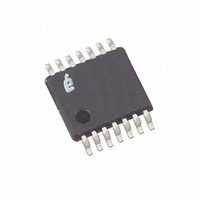
X95820WV14IZ-2.7T1 Intersil, X95820WV14IZ-2.7T1 Datasheet - Page 10

X95820WV14IZ-2.7T1
Manufacturer Part Number
X95820WV14IZ-2.7T1
Description
IC POT DGTL DUAL 10K OHM 14TSSOP
Manufacturer
Intersil
Series
XDCP™r
Datasheet
1.X95820WV14IZ-2.7T1.pdf
(12 pages)
Specifications of X95820WV14IZ-2.7T1
Taps
256
Resistance (ohms)
10K
Number Of Circuits
2
Temperature Coefficient
45 ppm/°C Typical
Memory Type
Non-Volatile
Interface
I²C, 2-Wire Serial
Voltage - Supply
2.7 V ~ 5.5 V
Operating Temperature
-40°C ~ 85°C
Mounting Type
Surface Mount
Package / Case
14-TSSOP
Resistance In Ohms
10K
Number Of Elements
2
# Of Taps
256
Resistance (max)
10KOhm
Power Supply Requirement
Single
Interface Type
Serial (I2C)
Single Supply Voltage (typ)
3.3V
Dual Supply Voltage (typ)
Not RequiredV
Single Supply Voltage (min)
2.7V
Single Supply Voltage (max)
5.5V
Dual Supply Voltage (min)
Not RequiredV
Dual Supply Voltage (max)
Not RequiredV
Operating Temp Range
-40C to 85C
Operating Temperature Classification
Industrial
Mounting
Surface Mount
Pin Count
14
Package Type
TSSOP
Lead Free Status / RoHS Status
Lead free / RoHS Compliant
Other names
X95820WV14IZ-2.7T1TR
Available stocks
Company
Part Number
Manufacturer
Quantity
Price
Part Number:
X95820WV14IZ-2.7T1
Manufacturer:
INTERSIL
Quantity:
20 000
All I
condition, which is a HIGH to LOW transition of SDA while
SCL is HIGH. The X95820 continuously monitors the SDA
and SCL lines for the START condition and does not
respond to any command until this condition is met (See
Figure 15). A START condition is ignored during the power
up sequence and during internal non-volatile write cycles.
All I
condition, which is a LOW to HIGH transition of SDA while
SCL is HIGH (See Figure 15). A STOP condition at the end
of a read operation, or at the end of a write operation to
volatile bytes only places the device in its standby mode. A
STOP condition during a write operation to a non-volatile
byte, initiates an internal non-volatile write cycle. The device
enters its standby state when the internal non-volatile write
cycle is completed.
An ACK, Acknowledge, is a software convention used to
indicate a successful data transfer. The transmitting device,
either master or slave, releases the SDA bus after
transmitting eight bits. During the ninth clock cycle, the
2
2
C interface operations must begin with a START
C interface operations must be terminated by a STOP
SDA
SCL
SDA Output from
SDA Output from
SCL from Master
Transmitter
Receiver
Signals from the
Signals from the
START
Signal at SDA
10
START
FIGURE 15. VALID DATA CHANGES, START, AND STOP CONDITIONS
Master
X95820
FIGURE 16. ACKNOWLEDGE RESPONSE FROM RECEIVER
High Impedance
S
a
t
r
t
FIGURE 17. BYTE WRITE SEQUENCE
1
STABLE
DATA
0
Identification
1
1
0
Byte
A2A1A0
CHANGE
DATA
X95820
0
Write
A
C
K
0 0 0 0
STABLE
DATA
receiver pulls the SDA line LOW to acknowledge the
reception of the eight bits of data (See Figure 16).
The X95820 responds with an ACK after recognition of a
START condition followed by a valid Identification Byte, and
once again after successful receipt of an Address Byte. The
X95820 also responds with an ACK after receiving a Data
Byte of a write operation. The master must respond with an
ACK after receiving a Data Byte of a read operation
A valid Identification Byte contains 1010 as the four MSBs,
and the following three bits matching the logic values
present at pins A2, A1, and A0. The LSB in the Read/Write
bit. Its value is “1” for a Read operation, and “0” for a Write
operation (See Table 2).
Address
Byte
(MSB)
1
TABLE 2. IDENTIFICATION BYTE FORMAT
0
A
C
K
8
Logic values at pins A2, A1, and A0 respectively
1
STOP
Data
Byte
0
ACK
High Impedance
9
A2
A
C
K
S
o
p
t
A1
A0
(LSB)
R/W
July 18, 2006
FN8212.2


