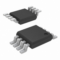
ISL95811UFUZ Intersil, ISL95811UFUZ Datasheet - Page 10

ISL95811UFUZ
Manufacturer Part Number
ISL95811UFUZ
Description
IC POT 256TAPS 5BYTES 8-MSOP
Manufacturer
Intersil
Series
XDCP™r
Datasheet
1.ISL95811WFUZ-T.pdf
(14 pages)
Specifications of ISL95811UFUZ
Taps
256
Resistance (ohms)
50K
Number Of Circuits
1
Temperature Coefficient
4 ppm/°C Typical
Memory Type
Non-Volatile
Interface
I²C, 2-Wire Serial
Voltage - Supply
2.7 V ~ 5.5 V
Operating Temperature
-40°C ~ 125°C
Mounting Type
Surface Mount
Package / Case
8-MSOP, Micro8™, 8-uMAX, 8-uSOP,
Resistance In Ohms
50K
Lead Free Status / RoHS Status
Lead free / RoHS Compliant
Available stocks
Company
Part Number
Manufacturer
Quantity
Price
Company:
Part Number:
ISL95811UFUZ
Manufacturer:
INTERSIL
Quantity:
13
either end of the array and between each resistor is an
electronic switch that transfers the potential at that point to
the wiper.
The electronic switches on the device operate in a “make
before break” mode when the wiper changes tap positions.
When the device is powered down, the last value stored in
IVR will be maintained in the non-volatile memory. When
power is restored, the contents of the IVR are recalled and
loaded into the WR to set the wiper to the initial value.
DCP Description
The DCP is implemented with a combination of resistor
elements and CMOS switches. The physical ends of each
DCP are equivalent to the fixed terminals of a mechanical
potentiometer (RH and RL pins). The RW pin of the DCP is
connected to intermediate nodes, and is equivalent to the
wiper terminal of a mechanical potentiometer. The position
of the wiper terminal within the DCP is controlled by an 8-bit
volatile Wiper Register (WR). When the WR of a DCP
contains all zeroes (WR[7:0] = 00h), its wiper terminal (RW)
is closest to its “Low” terminal (RL). When the WR register of
a DCP contains all ones (WR[7:0] = FFh), its wiper terminal
(RW) is closest to its “High” terminal (RH). As the value of
the WR increases from all zeroes (0) to all ones (255
decimal), the wiper moves monotonically from the position
closest to RL to the position closest to RH. At the same time,
the resistance between RW and RL increases monotonically,
while the resistance between RH and RW decreases
monotonically.
While the ISL95811 is being powered up, the WR is reset to
80h (128 decimal), which locates RW roughly at the center
between RL and RH. After the power supply voltage
becomes large enough for reliable non-volatile memory
reading, the WR will be reloaded with the value stored in a
non-volatile Initial Value Register (IVR).
The WR and IVR can be read or written to directly using the
I
Memory Description
The ISL95811 contains one non-volatile 8-bit Initial Value
Register (IVR), five General Purpose non-volatile 8-bit registers
and two volatile 8-bit registers: Wiper Register (WR) and
Access Control Register (ACR). The Memory map of the
ISL95811 is shown in Table 1. The non-volatile register (IVR) at
address 0 contains the initial wiper position and the volatile
register (WR) contains the current wiper position.
2
C serial interface, as described in the following sections.
10
ISL95811
The ISL95811 is pre-programed with 80h in the IVR.
The non-volatile IVR and volatile WR registers are
accessible with the same address.
The Access Control Register (ACR) contains information
and control bits described in Table 2.
The VOL bit (ACR[7]) determines whether the access to
wiper registers WR or initial value registers IVR.
If VOL bit is 0, the non-volatile IVR register and General
Purpose registers are accessible. If VOL bit is 1, only the
volatile WR is accessible. Note: Value written to the IVR
register is also written to the WR. The default value of this bit
is 0.
The Device ID register is read only and it contains chip
revision information, as shown in Table 3.
I
The ISL95811 supports a bidirectional bus oriented protocol.
The protocol defines any device that sends data onto the
bus as a transmitter and the receiving device as the receiver.
The device controlling the transfer is a master and the
device being controlled is the slave. The master always
initiates data transfers and provides the clock for both
transmit and receive operations. Therefore, the ISL95811
operates as a slave device in all applications.
All communication over the I
sending the MSB of each byte of data first.
VALUE
NAME
2
ADDRESS
BIT #
BIT #
C Serial Interface
(hex)
8
7
6
5
4
3
2
1
0
TABLE 2. ACCESS CONTROL REGISTER (ACR)
VOL
7
7
1
Device ID (read only)
TABLE 3. DEVICE ID REGISTER
General Purpose
General Purpose
General Purpose
General Purpose
General Purpose
NON-VOLATILE
6
0
6
0
TABLE 1. MEMORY MAP
IVR
NA
5
0
5
0
2
4
0
C interface is conducted by
4
0
Reserved
3
0
3
0
2
0
2
0
VOLATILE
ACR
N/A
N/A
N/A
N/A
N/A
N/A
WR
October 6, 2008
1
0
1
0
FN6759.1
0
0
0
0


