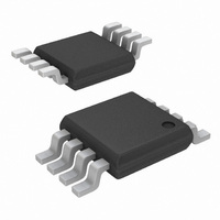
ISL95811UFUZ Intersil, ISL95811UFUZ Datasheet - Page 12

ISL95811UFUZ
Manufacturer Part Number
ISL95811UFUZ
Description
IC POT 256TAPS 5BYTES 8-MSOP
Manufacturer
Intersil
Series
XDCP™r
Datasheet
1.ISL95811WFUZ-T.pdf
(14 pages)
Specifications of ISL95811UFUZ
Taps
256
Resistance (ohms)
50K
Number Of Circuits
1
Temperature Coefficient
4 ppm/°C Typical
Memory Type
Non-Volatile
Interface
I²C, 2-Wire Serial
Voltage - Supply
2.7 V ~ 5.5 V
Operating Temperature
-40°C ~ 125°C
Mounting Type
Surface Mount
Package / Case
8-MSOP, Micro8™, 8-uMAX, 8-uSOP,
Resistance In Ohms
50K
Lead Free Status / RoHS Status
Lead free / RoHS Compliant
Available stocks
Company
Part Number
Manufacturer
Quantity
Price
Company:
Part Number:
ISL95811UFUZ
Manufacturer:
INTERSIL
Quantity:
13
Write Operation
A Write operation requires a START condition, followed by a
valid Identification Byte, a valid Address Byte, a Data Byte,
and a STOP condition. After each of the three bytes, the
ISL95811 responds with an ACK. At this time, if the Data
Byte is to be written only to volatile registers, then the device
enters its standby state. If the Data Byte is to be written also
to non-volatile memory, the ISL95811 begins its internal write
cycle to non-volatile memory. During the internal non-volatile
write cycle, the device ignores transitions at the SDA and
SCL pins, and the SDA output is at a high impedance state.
When the internal non-volatile write cycle is completed, the
ISL95811 enters its standby state (see Figure 19).
The byte at address 08h determines if the Data Byte is to be
written to volatile and/or non-volatile memory (see “Memory
Description” on page 10).
Data Protection
The WP pin has to be at logic HIGH to perform any Write
operation to the device. When the WP is active (LOW), the
device ignores Data Bytes of a Write Operation and does not
respond to the Data Bytes with an ACK; rather it goes into
standby state waiting for a new START condition.
A STOP condition also acts as a protection of non-volatile
memory. A valid Identification Byte, Address Byte, and total
number of SCL pulses act as a protection of both volatile
and non-volatile registers. During a Write sequence, the
Data Byte is loaded into an internal shift register as it is
SIGNAL AT SDA
FROM THE
SIGNALS
MASTER
SIGNALS FROM
THE SLAVE
S
T
A
R
T
0
IDENTIFICATION
1
BYTE WITH
SIGNALS FROM
SIGNAL AT SDA
SIGNALS FROM
0
R/W = 0
THE MASTER
THE ISL95811
1
12
0 0 0
0
A
C
K
0 0 0
ADDRESS
S
A
R
T
T
BYTE
0
FIGURE 19. BYTE WRITE SEQUENCE
0
IDENTIFICATION
1
FIGURE 20. READ SEQUENCE
0
BYTE
1
0
A
C
K
0
ISL95811
S
A
R
0
T
T
WRITE
0
0
IDENTIFICATION
A
C
K
1
BYTE WITH
0
R/W = 1
0 0 0 0
1
ADDRESS
received. If the Address Byte is 0 or 8, the Data Byte is
transferred to the Wiper Register (WR) or to the Access
Control Register respectively, at the falling edge of the SCL
pulse that loads the last bit (LSB) of the Data Byte. If the
Address Byte is 0, and the Access Control Register is all
zeros (default), then the STOP condition initiates the internal
write cycle to non-volatile memory.
Read Operation
A Read operation consists of a three byte instruction
followed by one or more Data Bytes (see Figure 20). The
master initiates the operation issuing the following
sequence: a START, the Identification byte with the R/W bit
set to “0”, an Address Byte, a second START, and a second
Identification byte with the R/W bit set to “1”. After each of
the three bytes, the ISL95811 responds with an ACK. The
ISL95811 then transmits the Data Byte and the master then
terminates the read operation (issuing a STOP condition)
following the last bit of the Data Byte.
The byte at address 08h determines if the Data Bytes being
read are from volatile or non-volatile memory (see “Memory
Description” on page 10).
0 0 0
BYTE
0
1
A
C
K
A
C
K
FIRST READ
DATA BYTE
DATA
BYTE
A
C
K
A
C
K
A
C
K
S
T
O
P
LAST READ
DATA BYTE
October 6, 2008
FN6759.1
O
S
T
P


