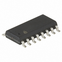
X9421YS16I-2.7 Intersil, X9421YS16I-2.7 Datasheet - Page 5

X9421YS16I-2.7
Manufacturer Part Number
X9421YS16I-2.7
Description
IC XDCP SGL 64-TAP 2.5K 16-SOIC
Manufacturer
Intersil
Series
XDCP™r
Datasheet
1.X9421WS16ZT1.pdf
(20 pages)
Specifications of X9421YS16I-2.7
Taps
64
Resistance (ohms)
2.5K
Number Of Circuits
1
Temperature Coefficient
300 ppm/°C Typical
Memory Type
Non-Volatile
Interface
SPI, 3-Wire Serial
Voltage - Supply
2.7 V ~ 5.5 V
Operating Temperature
-40°C ~ 85°C
Mounting Type
Surface Mount
Package / Case
16-SOIC (0.300", 7.5mm Width)
Resistance In Ohms
2.5K
Lead Free Status / RoHS Status
Contains lead / RoHS non-compliant
DEVICE ADDRESS (A
The address input is used to set the least significant bit of
the 8-bit slave address. A match in the slave address serial
data stream must be made with the address input in order to
initiate communication with the X9421. A maximum of two
devices may occupy the SPI serial bus.
Potentiometer Pins
V
The V
connections on either end of a mechanical potentiometer.
V
The wiper output is equivalent to the wiper output of a
mechanical potentiometer.
HARDWARE WRITE PROTECT INPUT (WP)
The WP pin when LOW prevents nonvolatile writes to the
Data Registers. Writing to the Wiper Counter Register is not
restricted.
SYSTEM/DIGITAL SUPPLY (V
VCC is the supply voltage for the system/digital section. VSS
is the system ground.
Principles of Operation
The X9421 is a highly integrated microcircuit incorporating a
resistor array and associated registers and counter and the
serial interface logic providing direct communication
between the host and the XDCP potentiometer.
Serial Interface
The X9421 supports the SPI interface hardware
conventions. The device is accessed via the SI input with
data clocked in on the rising SCK. CS must be LOW and the
HOLD and WP pins must be HIGH during the entire
operation.
The SO and SI pins can be connected together, since they
have three state outputs. This can help to reduce system pin
count.
Array Description
The X9421 is comprised of one resistor array containing 63
discrete resistive segments that are connected in series. The
physical ends of each array are equivalent to the fixed
terminals of a mechanical potentiometer (V
inputs).
At both ends of the array and between each resistor
segment is a CMOS switch connected to the wiper (V
output. Within the individual array only one switch may be
turned on at a time.
These switches are controlled by a Wiper Counter Register
(WCR). The six bits of the WCR are decoded to select, and
H
W
/R
/R
H
W
H
, V
/R
L
H
/R
and V
L
L
/R
L
inputs are equivalent to the terminal
0
)
5
CC
)
H
/R
H
and V
W
L
/R
/R
W
L
)
X9421
enable, one of sixty-four switches. The block diagram of the
potentiometer is shown in Figure 1.
Wiper Counter Register (WCR)
The X9421 contains a Wiper Counter Register. The WCR
can be envisioned as a 6-bit parallel and serial load counter
with its outputs decoded to select one of sixty-four switches
along its resistor array. The contents of the WCR can be
altered in four ways: it may be written directly by the host via
the Write Wiper Counter Register instruction (serial load); it
may be written indirectly by transferring the contents of one
of four associated Data Registers via the XFR Data Register
instruction (parallel load); it can be modified one step at a
time by the Increment/Decrement instruction. Finally, it is
loaded with the contents of its data register zero (DR0) upon
power-up.
The Wiper Counter Register is a volatile register; that is, its
contents are lost when the X9421 is powered-down.
Although the register is automatically loaded with the value
in DR0 upon power-up, this may be different from the value
present at power-down.
Data Registers
The potentiometer has four 6-bit nonvolatile Data Registers.
These can be read or written directly by the host. Data can
also be transferred between any of the four Data Registers
and the WCR. It should be noted all operations changing
data in one of the Data Registers is a nonvolatile operation
and will take a maximum of 10ms.
If the application does not require storage of multiple
settings for the potentiometer, the Data Registers can be
used as regular memory locations for system parameters or
user preference data.
Register Descriptions
There are four 6-bit Data Registers associated with the
potentiometer.
• {D5~D0}: These bits are for general purpose Nonvolatile
• {WP5~WP0}: These bits specify the wiper position of the
TABLE 2. WIPER COUNTER REGISTER, (6-BIT), VOLATILE
data storage or for storage of up to four different wiper
values.
potentiometer.
0
0
(MSB)
(MSB)
TABLE 1. DATA REGISTERS, (6-BIT), NONVOLATILE
0
0
WP5
D5
WP4
D4
WP3
D3
WP2
D2
WP1
D1
January 14, 2009
(LSB)
(LSB)
FN8196.4
WP0
D0


