X9421YS16I-2.7 Intersil, X9421YS16I-2.7 Datasheet - Page 7

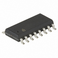
X9421YS16I-2.7
Manufacturer Part Number
X9421YS16I-2.7
Description
IC XDCP SGL 64-TAP 2.5K 16-SOIC
Manufacturer
Intersil
Series
XDCP™r
Datasheet
1.X9421WS16ZT1.pdf
(20 pages)
Specifications of X9421YS16I-2.7
Taps
64
Resistance (ohms)
2.5K
Number Of Circuits
1
Temperature Coefficient
300 ppm/°C Typical
Memory Type
Non-Volatile
Interface
SPI, 3-Wire Serial
Voltage - Supply
2.7 V ~ 5.5 V
Operating Temperature
-40°C ~ 85°C
Mounting Type
Surface Mount
Package / Case
16-SOIC (0.300", 7.5mm Width)
Resistance In Ohms
2.5K
Lead Free Status / RoHS Status
Contains lead / RoHS non-compliant
Two of the eight instructions are two bytes in length and end
with the transmission of the instruction byte. These
instructions are:
• XFR Data Register to Wiper Counter Register —This
• XFR Wiper Counter Register to Data Register—This
The basic sequence of the two byte instructions is illustrated
in Figure 4. These two-byte instructions exchange data
between the WCR and one of the Data Registers. A transfer
from a Data Register to a WCR is essentially a write to a static
RAM, with the static RAM controlling the wiper position. The
response of the wiper to this action will be delayed by t
transfer from the WCR (current wiper position), to a Data
Register is a write to nonvolatile memory and takes a
minimum of t
the potentiometer and one of its associated registers.
Five instructions require a three-byte sequence to complete.
These instructions transfer data between the host and the
X9421; either between the host and one of the Data
instruction transfers the contents of one specified Data
Register to the Wiper Counter Register.
instruction transfers the contents of the Wiper Counter
Register to the specified associated Data Register.
SCL
CS
SI
WR
0
SCK
to complete. The transfer can occur between
CS
SI
1
0
1
7
1
0
1
FIGURE 5. THREE-BYTE INSTRUCTION SEQUENCE (WRITE)
1
0
FIGURE 4. TWO-BYTE INSTRUCTION SEQUENCE
0
A0
1
1
I3
WRL
I2
1
. A
0
I1
X9421
I0
A0
R1 R0
I3
Registers or directly between the host and the WCR. These
instructions are:
• Read Wiper Counter Register—read the current wiper
• Write Wiper Counter Register—change current wiper
• Read Data Register—read the contents of the selected
• Write Data Register—write a new value to the selected
• Read Status—This command returns the contents of the
The sequence of these operations is shown in Figure 5 and
Figure 6.
The final command is Increment/Decrement. It is different
from the other commands, because it’s length is
indeterminate. Once the command is issued, the master can
clock the wiper up and/or down in one resistor segment step;
thereby, providing a fine tuning capability to the host. For
each SCK clock pulse (t
wiper will move one resistor segment towards the V
terminal. Similarly, for each SCK clock pulse while SI is
LOW, the selected wiper will move one resistor segment
towards the V
sequence and timing for this operation are shown in Figure 7
and 8.
position of the pot,
position of the pot,
data register;
data register.
WIP bit which indicates if the internal write cycle is in
progress.
I2
0
I1
0
I0
L
/R
R1
0
L
terminal. A detailed illustration of the
R0
0
HIGH
D5 D4
0
) while SI is HIGH, the selected
0
D3 D2
D1 D0
January 14, 2009
H
/R
FN8196.4
H


