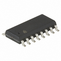
X9421YS16I-2.7 Intersil, X9421YS16I-2.7 Datasheet - Page 9

X9421YS16I-2.7
Manufacturer Part Number
X9421YS16I-2.7
Description
IC XDCP SGL 64-TAP 2.5K 16-SOIC
Manufacturer
Intersil
Series
XDCP™r
Datasheet
1.X9421WS16ZT1.pdf
(20 pages)
Specifications of X9421YS16I-2.7
Taps
64
Resistance (ohms)
2.5K
Number Of Circuits
1
Temperature Coefficient
300 ppm/°C Typical
Memory Type
Non-Volatile
Interface
SPI, 3-Wire Serial
Voltage - Supply
2.7 V ~ 5.5 V
Operating Temperature
-40°C ~ 85°C
Mounting Type
Surface Mount
Package / Case
16-SOIC (0.300", 7.5mm Width)
Resistance In Ohms
2.5K
Lead Free Status / RoHS Status
Contains lead / RoHS non-compliant
Read Wiper Counter Register
Write Wiper Counter Register
Read Data Register
Write Data Register
XFR Data Register to Wiper
Counter Register
XFR Wiper Counter Register to Data
Register
Increment/Decrement Wiper
Counter Register
Read Status (WIP bit)
Instruction Format
NOTES:
Read Wiper Counter Register (WCR)
Write Wiper Counter Register (WCR)
Read Data Register (DR)
Read the contents of the Register pointed to by R1 - R0.
Write Data Register (DR)
Write a new value to the Register pointed to by R1 - R0.
FALLING
FALLING
FALLING
FALLING
1. “A0”: stands for the device addresses sent by the master.
2. WPx refers to wiper position data in the Wiper Counter Register
3. “D”: stands for the decrement operation, SI held LOW during active SCK phase (high).
EDGE
EDGE
EDGE
EDGE
CS
CS
CS
“I”: stands for the increment operation, SI held HIGH during
active SCK phase (high).
CS
INSTRUCTION
0
0
0
IDENTIFIER
IDENTIFIER
0
IDENTIFIER
IDENTIFIER
DEVICE
DEVICE
DEVICE
DEVICE
TYPE
TYPE
TYPE
1
1
TYPE
1
1
0
0
0
0
1
1
1
1
ADDRESSES
1
1
1
1
ADDRESSES
ADDRESSES
ADDRESSES
DEVICE
DEVICE
DEVICE
DEVICE
1
1
1
1
9
I
1
1
1
1
1
1
0
0
3
0
0
0
0
A
0
A0
A0
A0
I
0
0
0
1
1
1
0
1
2
INSTRUCTION
1
INSTRUCTION
INSTRUCTION
1
1
1
OPCODE
INSTRUCTION
I
0
1
1
0
0
1
1
0
1
INSTRUCTION SET
OPCODE
1
OPCODE
OPCODE
0
0
0
0
I
1
0
1
0
1
0
0
1
0
1
1
TABLE 3. INSTRUCTION SET
0
0
1/0
1/0
1/0
1/0
R
0
1
0
0
0
0
1
1
ADDRESSES
R
1
REGISTER
R1
0
ADDRESSES
1/0
1/0
1/0
1/0
0
R
R
0
0
0
0
0
REGISTER
X9421
0
0
0
R0
0
0
0
0
0
0
0
0
0
0
0
0
0
0
0
0
0
0
0
0
0
0
0
0
0
1
0
0
0
0
Read the contents of the Wiper Counter Register
Write new value to the Wiper Counter Register
Read the contents of the Data Register pointed to by R
Write new value to the Data Register pointed to by R
Transfer the contents of the Data Register pointed to by R
R
Transfer the contents of the Wiper Counter
Register to the Data Register pointed to by R
Enable Increment/decrement of the Wiper Counter Register
Read the status of the internal write cycle, by checking the WIP
bit.
0
WP
(SENT BY HOST ON SI)
0
5
WP5
0
to the Wiper Counter Register
WP5
WP
WP5
DATA BYTE
4
(SENT BY HOST ON SI)
(SENT BY X9421 ON SO)
(SENT BY X9421 ON SO)
WP4
WP
WP4
WIPER POSITION
3
DATA BYTE
WP4 WP3
DATA BYTE
WP3
WP
2
WP3
WP
OPERATION
WP2
1
WP2
WP2
WP
0
WP1
WP1
WP1 WP0
RISING
EDGE
CS
WP0
WP0
1
January 14, 2009
- R
RISING
HIGH-VOLTAGE
EDGE
0
WRITE CYCLE
RISING
RISING
EDGE
EDGE
CS
CS
FN8196.4
CS
1
- R
1
- R
0
1
-
0


