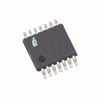
X95820WV14I-2.7 Intersil, X95820WV14I-2.7 Datasheet - Page 5

X95820WV14I-2.7
Manufacturer Part Number
X95820WV14I-2.7
Description
IC XDCP DUAL 256TAP 10K 14-TSSOP
Manufacturer
Intersil
Series
XDCP™r
Datasheet
1.X95820WV14IZ-2.7T1.pdf
(12 pages)
Specifications of X95820WV14I-2.7
Taps
256
Resistance (ohms)
10K
Number Of Circuits
2
Temperature Coefficient
45 ppm/°C Typical
Memory Type
Non-Volatile
Interface
I²C, 2-Wire Serial
Voltage - Supply
2.7 V ~ 5.5 V
Operating Temperature
-40°C ~ 85°C
Mounting Type
Surface Mount
Package / Case
14-TSSOP
Resistance In Ohms
10K
Number Of Elements
2
# Of Taps
256
Resistance (max)
10KOhm
Power Supply Requirement
Single
Interface Type
Serial (I2C)
Single Supply Voltage (typ)
3.3V
Dual Supply Voltage (typ)
Not RequiredV
Single Supply Voltage (min)
2.7V
Single Supply Voltage (max)
5.5V
Dual Supply Voltage (min)
Not RequiredV
Dual Supply Voltage (max)
Not RequiredV
Operating Temp Range
-40C to 85C
Operating Temperature Classification
Industrial
Mounting
Surface Mount
Pin Count
14
Package Type
TSSOP
Lead Free Status / RoHS Status
Contains lead / RoHS non-compliant
Operating Specifications
SDA vs. SCL Timing
WP, A0, A1, and A2 Pin Timing
Rpu (Note 15) SDA and SCL Bus Pull-up
(Notes 15, 16)
t
Cb (Note 15) Capacitive Loading of SDA
DH
t
t
R
F
SYMBOL
t
t
t
t
t
t
SU:WPA
HD:WPA
HD:DAT
SU:STO
HD:STO
(Note 15)
(Note 15)
SU:DAT
(Note 15) Output Data Hold Time
(OUTPUT TIMING)
t
(INPUT TIMING)
WP
WP, A0, A1, or A2
Input Data Setup Time
Input Data Hold Time
STOP Condition Setup Time From SCL rising edge crossing 70% of V
STOP Condition Setup Time From SDA rising edge to SCL falling edge. Both
SDA and SCL Rise Time
SDA and SCL Fall Time
or SCL
resIstor Off-chip
Non-volatile Write Cycle
Time
A2, A1, A0, and WP Setup
Time
A2, A1, A0, and WP Hold
Time
SDA
SCL
SDA
SDA IN
t
SU:STA
SCL
PARAMETER
5
START
Over the recommended operating conditions unless otherwise specified. (Continued)
t
HD:STA
t
F
t
From SDA exiting the 30% to 70% of V
window, to SCL rising edge crossing 30% of V
From SCL rising edge crossing 70% of V
entering the 30% to 70% of V
rising edge crossing 30% of V
crossing 70% of V
From SCL falling edge crossing 30% of V
SDA enters the 30% to 70% of V
From 30% to 70% of V
From 70% to 30% of V
Total on-chip and off-chip
Maximum is determined by t
For Cb = 400pF, max is about 2~2.5kΩ.
For Cb = 40pF, max is about 15~20kΩ.
Before START condition
After STOP condition
SU:WPA
t
SU:DAT
Clk 1
t
HIGH
TEST CONDITIONS
CC
X95820
.
CC
CC
t
LOW
R
CC
CC
and t
t
HD:DAT
.
CC
window.
F
window.
.
t
HD:WPA
CC
CC
CC
CC
, to SDA
t
to SDA
R
, until
CC
t
AA
STOP
0.1 * Cb
0.1 * Cb
20 +
20 +
MIN
t
100
600
600
600
600
10
DH
0
0
1
(Note 1)
TYP
12
t
BUF
MAX
250
250
400
t
20
SU:STO
July 18, 2006
UNITS
FN8212.2
kΩ
ms
pF
ns
ns
ns
ns
ns
ns
ns
ns
ns


