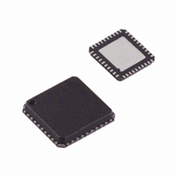
AD5405YCPZ Analog Devices Inc, AD5405YCPZ Datasheet - Page 7

AD5405YCPZ
Manufacturer Part Number
AD5405YCPZ
Description
IC DAC DUAL 12BIT MULT 40-LFCSP
Manufacturer
Analog Devices Inc
Datasheet
1.AD5405YCPZ.pdf
(24 pages)
Specifications of AD5405YCPZ
Data Interface
Parallel
Settling Time
80ns
Number Of Bits
12
Number Of Converters
2
Voltage Supply Source
Single Supply
Power Dissipation (max)
50µW
Operating Temperature
-40°C ~ 125°C
Mounting Type
Surface Mount
Package / Case
40-LFCSP
Resolution (bits)
12bit
Sampling Rate
21.3MSPS
Input Channel Type
Parallel
Supply Voltage Range - Analogue
2.5V To 5.5V
Supply Current
500nA
Digital Ic Case Style
CSP
Lead Free Status / RoHS Status
Lead free / RoHS Compliant
For Use With
EVAL-AD5405EB - BOARD EVAL FOR AD5405
Lead Free Status / RoHS Status
Lead free / RoHS Compliant, Lead free / RoHS Compliant
Available stocks
Company
Part Number
Manufacturer
Quantity
Price
Company:
Part Number:
AD5405YCPZ
Manufacturer:
Analog Devices Inc
Quantity:
1 779
Company:
Part Number:
AD5405YCPZ
Manufacturer:
Infineon
Quantity:
45
PIN CONFIGURATION AND FUNCTION DESCRIPTIONS
Table 4. Pin Function Descriptions
Pin No.
1 to 4
5, 26
6
7
8
9, 34 to 37
10 to 21
22
23
24
25
27 to 30
31, 40
32
33
38
39
Mnemonic
R1A, R2B,
R2_3B, R3A
V
DGND
LDAC
DAC A /B
NC
DB11 to DB0
CS
R/W
CLR
V
R3B, R2_3B,
R2B, R1B
R
I
I
I
I
EPAD
OUT
OUT
OUT
OUT
FB
REF
DD
B, R
2B
1B
1A
2A
A, V
FB
REF
A
B
Digital Ground Pin.
Not internally connected.
Parallel Data Bits 11 through 0.
Positive Power Supply Input. These parts can be operated from a supply of 2.5 V to 5.5 V.
Exposed pad must be connected to ground.
Description
DAC A 4-Quadrant Resistors. Allow a number of configuration modes, including bipolar operation with
minimum of external components.
DAC Reference Voltage Input Terminals.
Load DAC Input. Allows asynchronous or synchronous updates to the DAC output. The DAC is
asynchronously updated when this signal goes low. Alternatively, if this line is held permanently low, an
automatic or synchronous update mode is selected whereby the DAC is updated on the rising edge of CS.
Selects DAC A or B. Low selects DAC A, and high selects DAC B.
Chip Select Input. Active low. Used in conjunction with R/W to load parallel data to the input latch or to
read data from the DAC register. Edge sensitive; when pulled high, the DAC data is latched.
Read/Write. When low, used in conjunction with CS to load parallel data. When high, used in conjunction
with CS to read back contents of DAC register.
Active Low Control Input. Clears DAC output and input and DAC registers.
DAC B 4-Quadrant Resistors. Allow a number of configuration modes, including bipolar operation with a
minimum of external components.
External Amplifier Output.
DAC A Analog Ground. This pin typically should be tied to the analog ground of the system, but can be
biased to achieve single-supply operation.
DAC B Current Outputs.
DAC A Current Outputs.
DAC A Analog Ground. This pin typically should be tied to the analog ground of the system, but can be
biased to achieve single-supply operation.
NOTES
1. NC = NO CONNECT.
2. EXPOSED PAD MUST BE CONNECTED TO GROUND.
DAC A/B
R2_3A
V
DGND
LDAC
DB11
REF
R1A
R2A
R3A
NC
A
10
1
2
3
4
5
6
7
8
9
Figure 4. Pin Configuration
PIN 1
INDICATOR
Rev. B | Page 7 of 24
(Not to Scale)
AD5405
TOP VIEW
30 R1B
29 R2B
28 R2_3B
27 R3B
26 V
25 V
24 CLR
23 R/W
22 CS
21 DB0
REF
DD
B
AD5405


