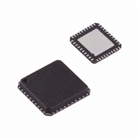
AD9717BCPZ Analog Devices Inc, AD9717BCPZ Datasheet - Page 33

AD9717BCPZ
Manufacturer Part Number
AD9717BCPZ
Description
IC DAC DUAL 14BIT LO PWR 40LFCSP
Manufacturer
Analog Devices Inc
Series
TxDAC®r
Datasheet
1.AD9717BCPZ.pdf
(80 pages)
Specifications of AD9717BCPZ
Data Interface
Serial
Number Of Bits
14
Number Of Converters
2
Voltage Supply Source
Analog and Digital
Power Dissipation (max)
86mW
Operating Temperature
-40°C ~ 85°C
Mounting Type
Surface Mount
Package / Case
40-LFCSP
Resolution (bits)
14bit
Sampling Rate
125MSPS
Input Channel Type
Parallel, Serial
Supply Current
11mA
Digital Ic Case Style
CSP
No. Of Pins
40
Lead Free Status / RoHS Status
Lead free / RoHS Compliant
Settling Time
-
Lead Free Status / RoHS Status
Lead free / RoHS Compliant, Lead free / RoHS Compliant
Available stocks
Company
Part Number
Manufacturer
Quantity
Price
Company:
Part Number:
AD9717BCPZ
Manufacturer:
ADI
Quantity:
172
Part Number:
AD9717BCPZ
Manufacturer:
ADI/亚德诺
Quantity:
20 000
SERIAL PERIPHERAL INTERFACE (SPI)
The serial port of the AD9714/AD9715/AD9716/AD9717 is a
flexible, synchronous serial communications port that allows easy
interfacing to many industry-standard microcontrollers and
microprocessors. The serial I/O is compatible with most synchron-
ous transfer formats, including both the Motorola SPI and Intel®
SSR protocols. The interface allows read/write access to all registers
that configure the AD9714/AD9715/AD9716/AD9717. Single or
multiple byte transfers are supported, as well as MSB first or
LSB first transfer formats. The serial interface port of the AD9714/
AD9715/AD9716/AD9717 is configured as a single I/O pin on
the SDIO pin.
GENERAL OPERATION OF THE SERIAL INTERFACE
There are two phases to a communications cycle on the AD9714/
AD9715/AD9716/AD9717. Phase 1 is the instruction cycle, which
is the writing of an instruction byte into the AD9714/AD9715/
AD9716/AD9717, coinciding with the first eight SCLK rising
edges. In Phase 2, the instruction byte provides the serial port
controller of the AD9714/AD9715/AD9716/AD9717 with infor-
mation regarding the data transfer cycle. The Phase 1 instruction
byte defines whether the upcoming data transfer is a read or write,
the number of bytes in the data transfer, and the starting register
address for the first byte of the data transfer. The first eight SCLK
rising edges of each communication cycle are used to write the
instruction byte into the AD9714/AD9715/AD9716/AD9717.
A Logic 1 on Pin 35 (RESET/PINMD), followed by a Logic 0,
resets the SPI port timing to the initial state of the instruction
cycle. This is true regardless of the present state of the internal
registers or the other signal levels present at the inputs to the
SPI port. If the SPI port is in the midst of an instruction cycle
or a data transfer cycle, none of the present data is written.
The remaining SCLK edges are for Phase 2 of the communication
cycle. Phase 2 is the actual data transfer between the AD9714/
AD9715/AD9716/AD9717 and the system controller. Phase 2 of
the communication cycle is a transfer of one, two, three, or four
data bytes, as determined by the instruction byte. Using one multi-
byte transfer is the preferred method. Single-byte data transfers
are useful to reduce CPU overhead when register access requires
one byte only. Registers change immediately upon writing to the
last bit of each transfer byte.
Rev. A | Page 33 of 80
INSTRUCTION BYTE
The instruction byte contains the information shown in Table 11.
Table 11.
MSB
DB7
R/W
R/ W (Bit 7 of the instruction byte) determines whether a read or a
write data transfer occurs after the instruction byte write. Logic 1
indicates a read operation. Logic 0 indicates a write operation.
N1 and N0 (Bit 6 and Bit 5 of the instruction byte) determine the
number of bytes to be transferred during the data transfer cycle.
The bit decodes are shown in Table 12.
Table 12. Byte Transfer Count
N1
0
0
1
1
A4, A3, A2, A1, and A0 (Bit 4, Bit 3, Bit 2, Bit 1, and Bit 0 of the
instruction byte) determine which register is accessed during the
data transfer portion of the communications cycle. For multi-
byte transfers, this address is the starting byte address. The
following register addresses are generated internally by the
AD9714/AD9715/AD9716/AD9717, based on the LSBFIRST bit
(Register 0x00, Bit 6).
SERIAL INTERFACE PORT PIN DESCRIPTIONS
SCLK—Serial Clock
The serial clock pin is used to synchronize data to and from the
AD9714/AD9715/AD9716/AD9717 and to run the internal state
machines. The SCLK maximum frequency is 20 MHz. All data
input to the AD9714/AD9715/AD9716/AD9717 is registered on
the rising edge of SCLK. All data is driven out of the AD9714/
AD9715/AD9716/AD9717 on the falling edge of SCLK.
CS —Chip Select
An active low input starts and gates a communications cycle.
It allows more than one device to be used on the same serial
communications lines. The SDIO/FORMAT pin reaches a
high impedance state when this input is high. Chip select
should stay low during the entire communications cycle.
SDIO—Serial Data I/O
The SDIO pin is used as a bidirectional data line to transmit
and receive data.
DB6
N1
AD9714/AD9715/AD9716/AD9717
N0
0
1
0
1
DB5
N0
Description
Transfer 1 byte
Transfer 2 bytes
Transfer 3 bytes
Transfer 4 bytes
DB4
A4
DB3
A3
DB2
A2
DB1
A1
LSB
DB0
A0


