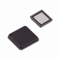
AD9717BCPZ Analog Devices Inc, AD9717BCPZ Datasheet - Page 46

AD9717BCPZ
Manufacturer Part Number
AD9717BCPZ
Description
IC DAC DUAL 14BIT LO PWR 40LFCSP
Manufacturer
Analog Devices Inc
Series
TxDAC®r
Datasheet
1.AD9717BCPZ.pdf
(80 pages)
Specifications of AD9717BCPZ
Data Interface
Serial
Number Of Bits
14
Number Of Converters
2
Voltage Supply Source
Analog and Digital
Power Dissipation (max)
86mW
Operating Temperature
-40°C ~ 85°C
Mounting Type
Surface Mount
Package / Case
40-LFCSP
Resolution (bits)
14bit
Sampling Rate
125MSPS
Input Channel Type
Parallel, Serial
Supply Current
11mA
Digital Ic Case Style
CSP
No. Of Pins
40
Lead Free Status / RoHS Status
Lead free / RoHS Compliant
Settling Time
-
Lead Free Status / RoHS Status
Lead free / RoHS Compliant, Lead free / RoHS Compliant
Available stocks
Company
Part Number
Manufacturer
Quantity
Price
Company:
Part Number:
AD9717BCPZ
Manufacturer:
ADI
Quantity:
172
Part Number:
AD9717BCPZ
Manufacturer:
ADI/亚德诺
Quantity:
20 000
AD9714/AD9715/AD9716/AD9717
COARSE GAIN ADJUSTMENT
Option 1
A coarse full-scale output current adjustment can be achieved
using the lower six bits in Register 0x0D. This adds or subtracts
up to 20% from the band gap voltage on Pin 34 (REFIO), and
the voltage on the FSADJx resistors tracks this change. As a
result, the DAC full-scale current varies by the same amount.
A secondary effect to changing the REFIO voltage is that the
full-scale voltage in the AUXDAC also changes by the same
magnitude. The register uses twos complement format, in
which 011111 maximizes the voltage on the REFIO node
and 100000 minimizes the voltage.
Option 2
While using the internal FSADJx resistors, each main DAC can
achieve independently controlled coarse gain using the lower
six bits of Register 0x04 (IRSET[5:0]) and Register 0x07
(QRSET[5:0]). Unlike Coarse Gain Option 1, this impacts only
the main DAC full-scale output current. The register uses twos
complement format and allows the output current to be changed
in approximately 0.25 dB steps.
1.30
1.25
1.20
1.15
1.10
1.05
1.00
0.95
0.90
0.85
0.80
4.0
3.5
3.0
2.5
2.0
1.5
1.0
0.5
0
0
0
Figure 98. Typical V
8
10
V
OUT
Figure 99. Effect of xR
_
16
Q
OR V
20
OUT
24
xR
_
I
SET
30
CODE
REF
32
CODE
Voltage vs. Code
SET
40
40
Code
48
50
56
60
Rev. A | Page 46 of 80
Option 3
Even when the device is in pin mode, full-scale values can be
adjusted by sourcing or sinking current from the FSADJx pins.
Any noise injected here appears as amplitude modulation of the
output. Thus, a portion of the required series resistance (at least
20 kΩ) must be installed right at the pin. A range of ±10% is
quite practical using this method.
Option 4
As in Option 3, when the device is in pin mode, both full-scale
values can be adjusted by sourcing or sinking current from the
REFIO pin. Noise injected here appears as amplitude modulation
of the output; therefore, a portion of the required series resis-
tance (at least 10 kΩ) must be installed at the pin. A range of
±25% is quite practical when using this method.
Fine Gain
Each main DAC has independent fine gain control using the
lower six bits in Register 0x03 (I DAC gain) and Register 0x06
(Q DAC gain). Unlike Coarse Gain Option 1, this impacts only
the main DAC full-scale output current. These registers use straight
binary format. One application in which straight binary format
is critical is for side-band suppression while using a quadrature
modulator. This is described in more detail in the Applications
Information section.
2.22
2.20
2.18
2.16
2.14
2.12
2.10
0
Figure 100. Typical DAC Gain Characteristics
8
3.3V DAC1
3.3V DAC2
1.8V DAC1
1.8V DAC2
16
24
GAIN DAC CODE
32
40
48
56
64


