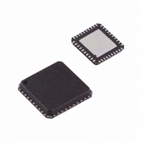
AD9717BCPZ Analog Devices Inc, AD9717BCPZ Datasheet - Page 39

AD9717BCPZ
Manufacturer Part Number
AD9717BCPZ
Description
IC DAC DUAL 14BIT LO PWR 40LFCSP
Manufacturer
Analog Devices Inc
Series
TxDAC®r
Datasheet
1.AD9717BCPZ.pdf
(80 pages)
Specifications of AD9717BCPZ
Data Interface
Serial
Number Of Bits
14
Number Of Converters
2
Voltage Supply Source
Analog and Digital
Power Dissipation (max)
86mW
Operating Temperature
-40°C ~ 85°C
Mounting Type
Surface Mount
Package / Case
40-LFCSP
Resolution (bits)
14bit
Sampling Rate
125MSPS
Input Channel Type
Parallel, Serial
Supply Current
11mA
Digital Ic Case Style
CSP
No. Of Pins
40
Lead Free Status / RoHS Status
Lead free / RoHS Compliant
Settling Time
-
Lead Free Status / RoHS Status
Lead free / RoHS Compliant, Lead free / RoHS Compliant
Available stocks
Company
Part Number
Manufacturer
Quantity
Price
Company:
Part Number:
AD9717BCPZ
Manufacturer:
ADI
Quantity:
172
Part Number:
AD9717BCPZ
Manufacturer:
ADI/亚德诺
Quantity:
20 000
Register
Memory R/W
CLKMODE
Version
Address
0x12
0x14
0x1F
Bit
7
6
4
3
2
1
0
7:6
4
3
2
1:0
7:0
Name
CALRSTQ
CALRSTI
CALEN
SMEMWR
SMEMRD
UNCALQ
UNCALI
CLKMODEQ[1:0]
Searching
Reacquire
CLKMODEN
CLKMODEI[1:0]
Version[7:0]
Description
0 (default): no action.
1: clear CALSTATQ.
0 (default): no action.
1: clear CALSTATI.
0 (default): no action.
1: initiate device self-calibration.
0 (default): no action.
1: write to static memory (calibration coefficients).
0 (default): no action.
1: read from static memory (calibration coefficients).
0 (default): no action.
1: reset Q DAC calibration coefficients to default (uncalibrated).
0 (default): no action.
1: reset I DAC calibration coefficients to default (uncalibrated).
Depending on the CLKMODEN bit setting, these two bits reflect the phase
relationship between DCLKIO and CLKIN, as described in Table 16.
If CLKMODEN = 0, read only; reports the clock phase chosen by the retimer.
If CLKMODEN = 1, read/write; value in this register sets Q clock phases; force if
needed to better synchronize the DACs (see the Retimer section).
Data path retimer status bit.
0 (default): clock relationship established.
1: indicates that the internal data path retimer is searching for clock relationship
(device output is not usable while this bit is high).
Edge triggered, 0 to 1 causes the retimer to reacquire the clock relationship.
0 (default): CLKMODEI/CLKMODEQ values computed by the two retimers and
read back in CLKMODEI[1:0] and CLKMODEQ[1:0].
1: CLKMODE values set in CLKMODEI[1:0] override both I and Q retimers.
Depending on CLKMODEN bit setting, these two bits reflect the phase
relationship between DCLKIO and CLKIN as described in Table 16.
If CLKMODEN = 0, read only; reports the clock phase chosen by the retimer.
If CLKMODEN = 1, read/write; value in this register sets I clock phases; force if
needed to better synchronize the DACs (see the Retimer section).
Hardware version of the device. This register is set to 0x03 for the latest version of
the device.
Rev. A | Page 39 of 80
AD9714/AD9715/AD9716/AD9717


