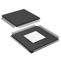
AD9785BSVZ Analog Devices Inc, AD9785BSVZ Datasheet - Page 35

AD9785BSVZ
Manufacturer Part Number
AD9785BSVZ
Description
IC DAC 12BIT 800MSPS 100TQFP
Manufacturer
Analog Devices Inc
Series
TxDAC®r
Datasheet
1.AD9785BSVZ.pdf
(64 pages)
Specifications of AD9785BSVZ
Data Interface
Serial
Number Of Bits
12
Number Of Converters
2
Voltage Supply Source
Analog and Digital
Power Dissipation (max)
450mW
Operating Temperature
-40°C ~ 85°C
Mounting Type
Surface Mount
Package / Case
100-TQFP Exposed Pad, 100-eTQFP, 100-HTQFP, 100-VQFP
Resolution (bits)
12bit
Sampling Rate
800MSPS
Input Channel Type
Parallel
Digital Ic Case Style
QFP
No. Of Pins
100
Operating Temperature Range
-40°C To +85°C
Lead Free Status / RoHS Status
Lead free / RoHS Compliant
Settling Time
-
Lead Free Status / RoHS Status
Lead free / RoHS Compliant, Lead free / RoHS Compliant
Available stocks
Company
Part Number
Manufacturer
Quantity
Price
Company:
Part Number:
AD9785BSVZ
Manufacturer:
Analog Devices Inc
Quantity:
135
Company:
Part Number:
AD9785BSVZ
Manufacturer:
Analog Devices Inc
Quantity:
10 000
Company:
Part Number:
AD9785BSVZRL
Manufacturer:
Analog Devices Inc
Quantity:
10 000
Setting the Frequency of DATACLK
The DATACLK signal is derived from the internal DAC sample
clock, DACCLK. The frequency of DATACLK output depends
on several programmable settings. The relationship between the
frequency of DACCLK and DATACLK is
where the variables have the values shown in Table 26.
Table 26. DACCLK to DATACLK Divisor Values
Variable
IF
P
f
DATACLK
Value
Interpolation factor
0.5 (if single port is enabled)
1 (if dual port is selected)
f
IF
DACCLK
P
DACCLK
DACCLK
REFCLK
REFCLK
SYNC_I
SYNC_I
INPUT
INPUT
DATA
DATA
Register
0x01
0x01
Address
t
S_SYNC
t
H_SYNC
Bits
[7:6]
[4]
Figure 49. REFCLK 2×
Figure 50. REFCLK 4×
Rev. A | Page 35 of 64
t
S_SYNC
t
SREFCLK
t
t
H_SYNC
SREFCLK
INPUT DATA REFERENCED TO REFCLK
In some systems, it may be more convenient to use the REFCLK
input instead of the DATACLK output as the input data timing
reference. If the frequency of DACCLK is equal to the frequency
of the data input (PLL is bypassed and no interpolation is used),
the timing parameter “Data with respect to REFCLK” shown in
Table 25 applies directly without further considerations. If the
frequency of DACCLK is greater than the frequency of the data
input, a divider is used to generate the internal data sampling clock
(DCLK_SMP). This divider creates a phase ambiguity between
REFCLK and DCLK_SMP, which, in turn, causes a sampling
time uncertainty. To establish fixed setup and hold times for the
data interface, this phase ambiguity must be eliminated.
To eliminate the phase ambiguity, the SYNC_I input pins
(Pin 13 and Pin 14) must be used to synchronize the data to
a specific DCLK_SMP phase. The specific steps for accom-
plishing this are detailed in the Device Synchronization section.
The timing relationships between SYNC_I, DACCLK, REFCLK,
and the input data are shown in Figure 49 through Figure 51.
t
HREFCLK
t
HREFCLK
AD9785/AD9787/AD9788


