AD5390BSTZ-5 Analog Devices Inc, AD5390BSTZ-5 Datasheet - Page 26
AD5390BSTZ-5
Manufacturer Part Number
AD5390BSTZ-5
Description
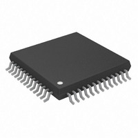
IC DAC 14BIT I2C 16CH 52-LQFP
Manufacturer
Analog Devices Inc
Specifications of AD5390BSTZ-5
Data Interface
I²C, Serial
Design Resources
8 to 16 Channels of Programmable Voltage with Excellent Temperature Drift Performance Using AD5390/1/2 (CN0029) AD5390/91/92 Channel Monitor Function (CN0030)
Settling Time
8µs
Number Of Bits
14
Number Of Converters
16
Voltage Supply Source
Single Supply
Power Dissipation (max)
35mW
Operating Temperature
-40°C ~ 85°C
Mounting Type
Surface Mount
Package / Case
52-LQFP
Resolution (bits)
14bit
Sampling Rate
125kSPS
Input Channel Type
Serial
Supply Voltage Range - Analogue
4.5V To 5.5V
Supply Voltage Range - Digital
2.7V To 5.5V
Lead Free Status / RoHS Status
Lead free / RoHS Compliant
For Use With
EVAL-AD5390EBZ - BOARD EVALUATION FOR AD5390
Lead Free Status / RoHS Status
Lead free / RoHS Compliant, Lead free / RoHS Compliant
Available stocks
Company
Part Number
Manufacturer
Quantity
Price
Company:

Part Number:
AD5390BSTZ-5
Manufacturer:
Analog Devices Inc
Quantity:
10 000


AD5390/AD5391/AD5392
Standalone Mode
By connecting the daisy-chain enable (DCEN) pin low,
standalone mode is enabled. The serial interface works with
both a continuous and a noncontinuous serial clock. The first
falling edge of SYNC starts the write cycle and resets a counter
that counts the number of serial clocks to ensure that the
correct number of bits is shifted into the serial shift register.
Any further edges on SYNC except for a falling edge are
ignored until 24 bits are clocked in. Once 24 bits have been
shifted in, the SCLK is ignored. For another serial transfer to
take place, the counter must be reset by the falling edge of
SYNC .
Daisy-Chain Mode
For systems that contain several devices, the SDO pin can be
used to daisy-chain the devices together. This daisy-chain mode
can be useful in system diagnostics and for reducing the
number of serial interface lines.
By connecting the DCEN pin high, daisy-chain mode is
enabled. The first falling edge of SYNC starts the write cycle.
The SCLK is continuously applied to the input shift register
when SYNC is low. If more than 24 clock pulses are applied,
the data ripples out of the shift register and appears on the SDO
line. This data is clocked out on the rising edge of SCLK and is
valid on the falling edge. By connecting the SDO of the first
device to the DIN input on the next device in the chain, a
multidevice interface is constructed. For each device in the
system, 24 clock pulses are required. Therefore, the total
number of clock cycles must equal 24N where N is the total
number of AD539x devices in the chain.
When the serial transfer to all devices is complete, SYNC is
taken high. This latches the input data in each device in the
daisy chain and prevents any further data from being clocked
into the input shift register.
SYNC
SCLK
SDO
DIN
INPUT WORD SPECIFIES REGISTER TO BE READ
DB23
DB23
UNDEFINED
Figure 32. AD539x Readback Operation
24
DB0
DB0
Rev. A | Page 26 of 44
DB23
DB23
SELECTED REGISTER DATA CLOCKED OUT
If SYNC is taken high before 24 clocks are clocked into the part,
it is considered a bad frame and the data is discarded.
The serial clock can be either a continuous or a gated clock. A
continuous SCLK source can be used only if the SYNC can be
held low for the correct number of clock cycles. In gated clock
mode, a burst clock containing the exact number of clock cycles
must be used and SYNC taken high after the final clock to latch
the data.
Readback Mode
Readback mode is invoked by setting the R/ W bit = 1 in the
serial input register write sequence. With R/ W = 1, Bits A3 to A0
in association with Bits REG1 and REG0 select the register to be
read. The remaining data bits in the write sequence are don’t
care bits. During the next SPI write, the data appearing on the
SDO output contains the data from the previously addressed
register. For a read of a single register, the NOP command can
be used in clocking out the data from the selected register on
SDO.
The readback diagram in Figure 32 shows the readback
sequence. For example, to read back the m register of Channel 0
on the AD539x, the following sequence should be implemented.
First, write 0x404XXX to the AD539x input register. This
configures the AD539x for read mode with the m register of
Channel 0 selected. Note that all Data Bits DB13 to DB0 are
don’t care bits. Follow this with a second write, a NOP
condition, and 0x000000. During this write, the data from the m
register is clocked out on the DOUT line—that is, data clocked
out contains the data from the m register in Bits DB13 to DB0,
and the top 10 bits contain the address information as
previously written. In readback mode, the SYNC signal must
frame the data. Data is clocked out on the rising edge of SCLK
and is valid on the falling edge of the SCLK signal. If the SCLK
idles high between the write and read operations of a readback,
then the first bit of data is clocked out on the falling edge of
SYNC .
NOP CONDITION
48
DB0
DB0
Related parts for AD5390BSTZ-5
Image
Part Number
Description
Manufacturer
Datasheet
Request
R

Part Number:
Description:
Wideband Dual-Channel Linear Multiplier/Divider
Manufacturer:
AD [Analog Devices]
Datasheet:

Part Number:
Description:
±1.7g Dual-Axis IMEMS Accelerometer Evaluation Board
Manufacturer:
Analog Devices Inc
Datasheet:

Part Number:
Description:
Inertial Sensor Evaluation System
Manufacturer:
Analog Devices Inc
Datasheet:
Part Number:
Description:
Manufacturer:
Analog Devices Inc
Datasheet:
Part Number:
Description:
Manufacturer:
Analog Devices Inc
Datasheet:
Part Number:
Description:
Manufacturer:
Analog Devices Inc
Datasheet:
Part Number:
Description:
Manufacturer:
Analog Devices Inc
Datasheet:
Part Number:
Description:
Manufacturer:
Analog Devices Inc
Datasheet:
Part Number:
Description:
Manufacturer:
Analog Devices Inc
Datasheet:
Part Number:
Description:
Manufacturer:
Analog Devices Inc
Datasheet:
Part Number:
Description:
Manufacturer:
Analog Devices Inc
Datasheet:
Part Number:
Description:
Manufacturer:
Analog Devices Inc
Datasheet:
Part Number:
Description:
Manufacturer:
Analog Devices Inc
Datasheet: