AD5390BSTZ-5 Analog Devices Inc, AD5390BSTZ-5 Datasheet - Page 27
AD5390BSTZ-5
Manufacturer Part Number
AD5390BSTZ-5
Description
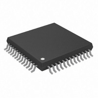
IC DAC 14BIT I2C 16CH 52-LQFP
Manufacturer
Analog Devices Inc
Specifications of AD5390BSTZ-5
Data Interface
I²C, Serial
Design Resources
8 to 16 Channels of Programmable Voltage with Excellent Temperature Drift Performance Using AD5390/1/2 (CN0029) AD5390/91/92 Channel Monitor Function (CN0030)
Settling Time
8µs
Number Of Bits
14
Number Of Converters
16
Voltage Supply Source
Single Supply
Power Dissipation (max)
35mW
Operating Temperature
-40°C ~ 85°C
Mounting Type
Surface Mount
Package / Case
52-LQFP
Resolution (bits)
14bit
Sampling Rate
125kSPS
Input Channel Type
Serial
Supply Voltage Range - Analogue
4.5V To 5.5V
Supply Voltage Range - Digital
2.7V To 5.5V
Lead Free Status / RoHS Status
Lead free / RoHS Compliant
For Use With
EVAL-AD5390EBZ - BOARD EVALUATION FOR AD5390
Lead Free Status / RoHS Status
Lead free / RoHS Compliant, Lead free / RoHS Compliant
Available stocks
Company
Part Number
Manufacturer
Quantity
Price
Company:

Part Number:
AD5390BSTZ-5
Manufacturer:
Analog Devices Inc
Quantity:
10 000


I
The AD5390/AD5391/AD5392 products feature an I
compatible 2-wire interface consisting of a serial data line
(SDA) and a serial clock line (SCL). SDA and SCL facilitate
communication between the DACs and the master at rates up
to 400 kHz. Figure 4 shows the 2-wire interface timing diagram.
When selecting the I
SPI/ I
as a slave device (that is, no clock is generated by the device).
The AD5390/AD5391/AD5392 have a 7-bit slave address
1010 1(AD1)(AD0). The five MSBs are hard-coded and the
two LSBs are determined by the state of the AD1 and AD0
pins. The hardware configuration facility for the AD1 and AD0
pins allows four of these devices to be configured on the bus.
I
One data bit is transferred during each SCL clock cycle. The
data on SDA must remain stable during the high period of the
SCL clock pulse. Changes in SDA while SCL is high are control
signals that configure START and STOP Conditions. Both SDA
and SCL are pulled high by the external pull-up resistors when
the I
START AND STOP CONDITIONS
A master device initiates communication by issuing a START
condition. A START condition is a high-to-low transition on
SDA with SCL high. A STOP condition is a low-to-high
transition on SDA, while SCL is high. A START condition from
the master signals the beginning of a transmission to the
AD539x. The STOP condition frees the bus. If a repeated
START condition (Sr) is generated instead of a STOP condition,
the bus remains active.
2
2
C DATA TRANSFER
C SERIAL INTERFACE
2
2
C bus is not busy.
C pin to Logic 0, the device is connected to the I
2
C operating mode by configuring the
2
C-
2
C bus
Rev. A | Page 27 of 44
REPEATED START CONDITION
A repeated START (Sr) condition may indicate a change of data
direction on the bus. Sr may be used when the bus master is
writing to several I
control of the bus.
ACKNOWLEDGE BIT (ACK)
The acknowledge bit (ACK) is the ninth bit attached to any
8-bit data-word. An ACK is always generated by the receiving
device. The AD539x devices generate an ACK when receiving
an address or data by pulling SDA low during the ninth clock
period.
Monitoring the ACK allows for detection of unsuccessful data
transfers. An unsuccessful data transfer occurs if a receiving
device is busy or if a system fault has occurred. In the event of
an unsuccessful data transfer, the bus master should reattempt
communication.
AD539x SLAVE ADDRESSES
A bus master initiates communication with a slave device by
issuing a START condition followed by the 7-bit slave address.
When idle, the AD539x device waits for a START condition
followed by its slave address. The LSB of the address word is the
read/write (R/ W ) bit. The AD539x devices are receive devices
only, and R/ W = 0 when communicating with them. After
receiving the proper address 1010 1(AD1) (AD0), the AD539x
issues an ACK by pulling SDA low for one clock cycle. The
AD539x has four user-programmable addresses determined by
the AD1 and AD0 bits.
2
C devices and does not want to relinquish
AD5390/AD5391/AD5392
Related parts for AD5390BSTZ-5
Image
Part Number
Description
Manufacturer
Datasheet
Request
R

Part Number:
Description:
Wideband Dual-Channel Linear Multiplier/Divider
Manufacturer:
AD [Analog Devices]
Datasheet:

Part Number:
Description:
±1.7g Dual-Axis IMEMS Accelerometer Evaluation Board
Manufacturer:
Analog Devices Inc
Datasheet:

Part Number:
Description:
Inertial Sensor Evaluation System
Manufacturer:
Analog Devices Inc
Datasheet:
Part Number:
Description:
Manufacturer:
Analog Devices Inc
Datasheet:
Part Number:
Description:
Manufacturer:
Analog Devices Inc
Datasheet:
Part Number:
Description:
Manufacturer:
Analog Devices Inc
Datasheet:
Part Number:
Description:
Manufacturer:
Analog Devices Inc
Datasheet:
Part Number:
Description:
Manufacturer:
Analog Devices Inc
Datasheet:
Part Number:
Description:
Manufacturer:
Analog Devices Inc
Datasheet:
Part Number:
Description:
Manufacturer:
Analog Devices Inc
Datasheet:
Part Number:
Description:
Manufacturer:
Analog Devices Inc
Datasheet:
Part Number:
Description:
Manufacturer:
Analog Devices Inc
Datasheet:
Part Number:
Description:
Manufacturer:
Analog Devices Inc
Datasheet: